Data sheet, Pin configuration, Pin description – Diodes AP1682 User Manual
Page 2
Data Sheet
Single Stage Primary Side Regulation PFC Controller For LED Driver AP1682
Dec. 2011 Rev. 1. 1 BCD Semiconductor Manufacturing Limited
2
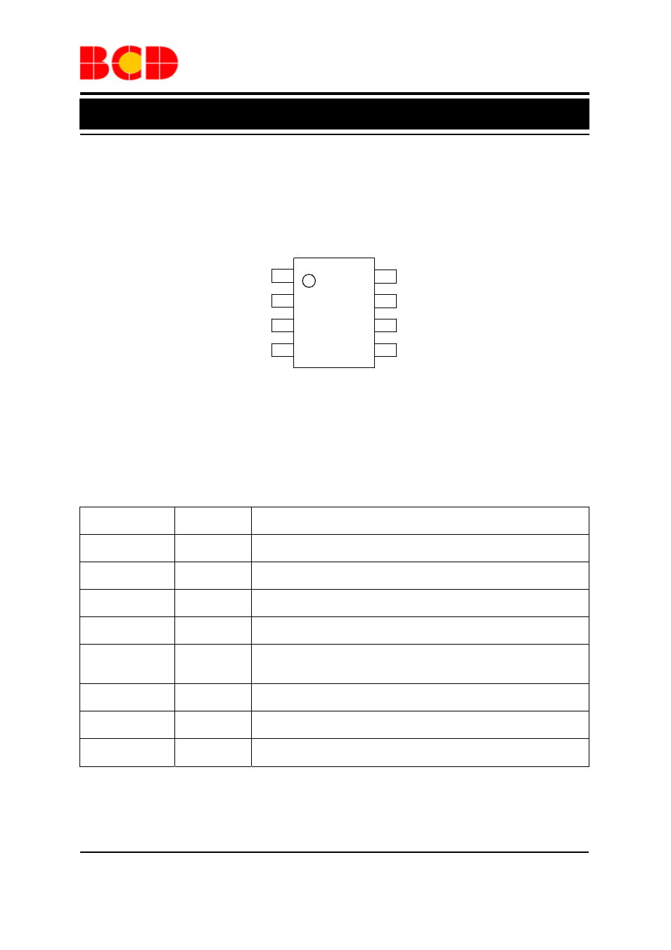
Pin Configuration
M Package
(SOIC-8)
Figure 2. Pin Configuration of AP1682 (Top View)
Pin Description
Pin Number
Pin Name
Function
1
NC No
connection
2
VS
The rectified input voltage sensing pin. The pin is detecting the
instantaneous rectified sine waveform of input voltage
3
VPK
The rectified input voltage peak value sensing pin. The pin is detecting
the rectified sine waveform peak value of input voltage
4
CS
Primary current sensing
5
FB
This pin captures the feedback voltage from the auxiliary winding. FB
voltage is used to control no load output voltage and determine
acceleration stop point at start-up phase
6
GND
Ground. Current return for gate driver and control circuits of the IC
7
OUT Gate
driver
output
8
VCC
Supply voltage of gate driver and control circuits of the IC
1
2
3
4
8
7
6
5
NC
VS
VPK
CS
FB
GND
OUT
VCC