Data sheet, High performance power factor corrector ap1662, Electrical characteristics (continued) – Diodes AP1662 User Manual
Page 7
Data Sheet
HIGH PERFORMANCE POWER FACTOR CORRECTOR AP1662
Jul. 2012 Rev. 1. 3 BCD Semiconductor Manufacturing Limited
7
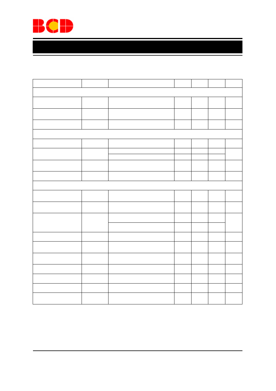
Electrical Characteristics (Continued)
V
CC
=12V, T
J
=-25°C to 125°C, C
O
=1nF, unless otherwise specified.
Parameter Symbol
Test
Conditions
Min
Typ
Max
Unit
Multiplier Section
Linear Input Voltage
Range
V
MULT
0 to 3
0 to
3.5
V
Output Maximum
Slope
△
V
CS
/
△
V
MULT
V
MULT
: 0 to 0.5V,
V
COMP
=Upper Clamp Voltage
1.65
1.9
Gain k
V
MULT
=1V, V
COMP
=4V 0.6
0.75
0.9
1/V
Current Sense Section
Input Bias Current
I
CS
V
CS
=0V
-1
µA
Current Sense Offset
Voltage
V
CS-OFFSET
V
MULT
=0V
30
mV
V
MULT
=2.5V
5
Current Sense
Reference Clamp
V
CS-CLAMP
V
COMP
= Upper Clamp
Voltage, V
MULT
= 2.5V
1.6 1.7 1.8 V
Delay to Output
t
d(H-L
)
200
350
ns
Zero Current Detection Section
Arming Voltage
(positive-going edge)
V
ZCDA
(Note
2)
2.1
V
Triggering Voltage
(negative-going edge)
V
ZCDT
(Note
2)
1.6
V
Upper Clamp Voltage
V
ZCD-H
I
ZCD
=20µA 4.5
5.1
5.9
V
I
ZCD
=3mA 4.7
5.2
6.1
Lower Clamp Voltage
V
ZCD-L
I
ZCD
= -3mA
0.3
0.65
1
V
Source Current
Capability
I
ZCD-SR
-2.5 -10 mA
Sink Current
Capability
I
ZCD-SN
3
mA
Sink Bias Current
I
ZCD-B
1V
≤ V
ZCD
≤ 4.5 V
2
µA
Disable Threshold
V
ZCD-DIS
150 200 250 mV
Disable Hysteresis
V
ZCD-HYS
100
mV
Restart Current After
Disable
I
ZCD-RES
V
ZCD
DIS , V CC >V CC-OFF -80 -120 µA
Note 2: Limits over the full temperature are guaranteed by design, but not tested in production.