Ap7217a, Electrical characteristics, 3v 600ma cmos ldo – Diodes AP7217A User Manual
Page 4
AP7217A
3.3V 600mA CMOS LDO
AP7217A Rev. 3
4 of 10
OCTOBER 2009
DS31423
©
Diodes Incorporated
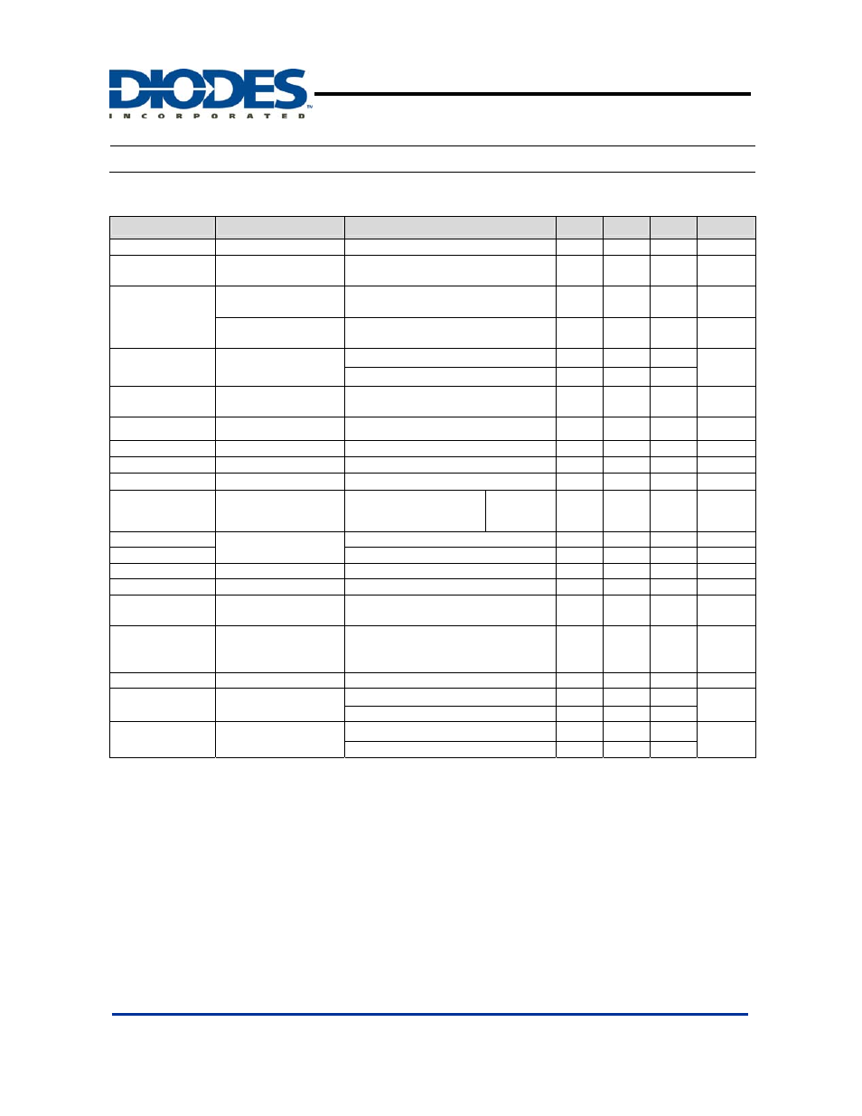
Electrical Characteristics
(T
A
= 25
°C, C
IN
= 1µF, C
OUT
= 1µF, V
EN
= V
IN
, unless otherwise noted)
Symbol
Parameter
Test Conditions
Min
Typ.
Max
Unit
I
Q
Quiescent
Current
I
O
= 0mA
-
50
80
µA
I
STB
Standby
Current
V
EN
= Off
V
IN
= 5.0V
15 25 µA
Output Voltage
Accuracy
I
O
= 30mA, V
IN
= 5V
3.234
3.300 3.366
V
VR
OUT
V
OUT
Temperature
Coefficient
-40
°C to 85°C, I
OUT
= 30mA
±100
ppm
/
o
C
I
OUT
= 300mA
350
400
V
DROPOUT
Dropout
Voltage
I
OUT
= 600mA
800
900
mV
I
OUT
Maximum Output
Current
V
IN
= 5.3V
600
mA
I
LIMIT
Current
Limit V
IN
= 5.3V
750
mA
I
short
Short Circuit Current V
IN
= 5.3V
50
mA
∆V
LINE
/
∆V
IN
/V
OUT
Line Regulation
4.3V
≤ V
IN
≤ 5.5V; I
OUT
= 30mA
0.01
±0.2
%/V
∆V
OUT
Load Regulation
1mA
≤ I
OUT
≤ 100mA, V
IN
= 5.3V
15
50
mV
PSRR
Power Supply
Rejection
V
IN
=
4.3V+ 0.5Vp-pAC,
I
OUT
= 50mA
F = 1KHz
55
dB
V
EH
Output
ON
1.6
V
V
EL
EN Input Threshold
Output OFF
0.25
V
I
EN
Enable Pin Current
-0.1
0.1
µA
V
DF
Detect fall voltage
3.23
3.3
3.37
V
V
D
Hysteresis
Range
V
Hysteresis
V
DF
x1.02
V
DF
x1.05
V
DF
x1.08
V
I
VDout
VD Supply Current
VDout = 0.5V
V
IN
= 2.0V
3.0V
20
30
mA
t
RP
V
DOUT
Delay Time
V
IN
= 1.8V to VDF+ 1V
180
200
-
mSec
SOP-8L (Note 3)
134
θ
JA
Thermal Resistance
Junction-to-Ambient SOP-8L-EP (Note 4)
82
ºC/W
SOP-8L (Note 3)
28
θ
JC
Thermal Resistance
Junction-to-Case
SOP-8L-EP (Note 4)
12
ºC/W
Notes: 3. Test condition for SOP-8L: Device mounted on FR-4 substrate PC board, 2oz copper, with minimum recommended pad layout.
4. Test condition for SOP-8L-EP: Device mounted on 2oz copper, minimum recommended pad layout on top & bottom layer with thermal vias,
double sided FR-4 PCB.