Data sheet, Recommended operating conditions – Diodes AP2132B User Manual
Page 5
Data Sheet
2A CMOS LDO REGULATOR AP2132B
Oct. 2012
Rev. 1. 1 BCD Semiconductor Manufacturing Limited
5
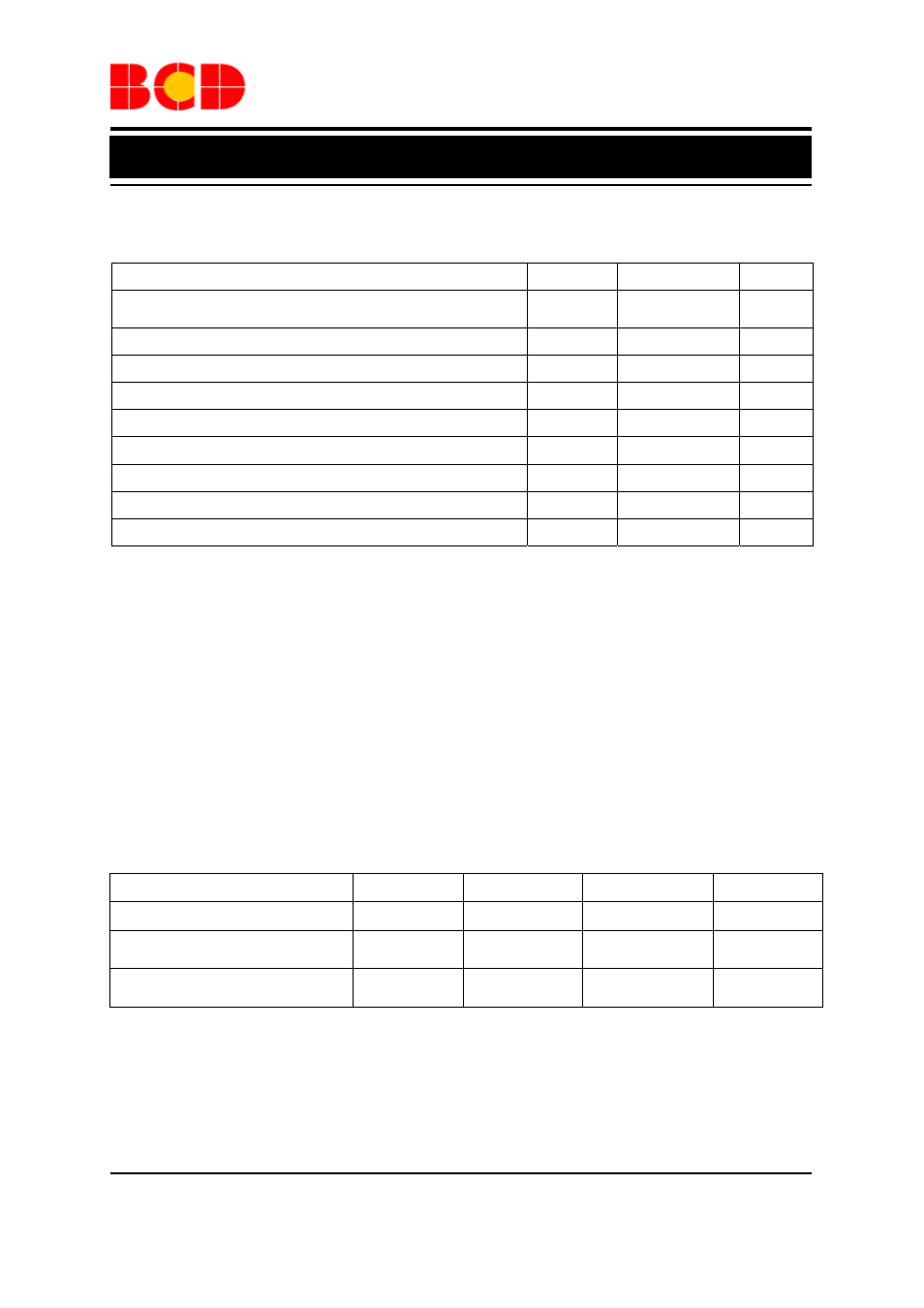
Absolute Maximum Ratings (Note 1)
Note 1: Stresses greater than those listed under “Absolute Maximum Ratings” may cause permanent damage to
the device. These are stress ratings only and functional operation of the device at these or any other conditions
beyond those indicated under “Recommended Operating Conditions” is not implied. Exposure to “Absolute
Maximum Ratings” for extended periods may affect device reliability.
Note 2:
θ
JA
is measured with the component mounted on 2-Layer FR-4 PCB board with 1.0cm*1.0cm thermal
sink pad in free air.
Recommended Operating Conditions
Parameter
Symbol Min
Max Unit
Input Voltage
V
IN
1.4 5.5 V
Input Voltage for Controlling
Circuit
V
CTRL
4.5
5.5
V
Operating Ambient Temperature
Range
T
A
-40 85 °C
Parameter
Symbol Value Unit
Input Voltage
Input Voltage for Controlling Circuit
V
IN
V
CTRL
6.0 V
Enable Input Voltage
V
EN
-0.3 to 6.0
V
Output Current
I
OUT
2.5 A
Thermal Resistance (Note 2)
θ
JA
53 ºC/W
Operating Junction Temperature
T
J
150
ºC
Storage Temperature Range
T
STG
-65
to
150 ºC
Lead Temperature (Soldering, 10sec)
T
LEAD
260 ºC
ESD (Machine Model)
200
V
ESD (Human Body Model)
2000
V