Ap139, Typical performance characteristics, Functional description – Diodes AP139 User Manual
Page 5: 300ma low-noise cmos ldo
AP139
300mA LOW-NOISE CMOS LDO
AP139 Rev. 6
5 of 7
FEBRUARY 2009
©
Diodes Incorporated
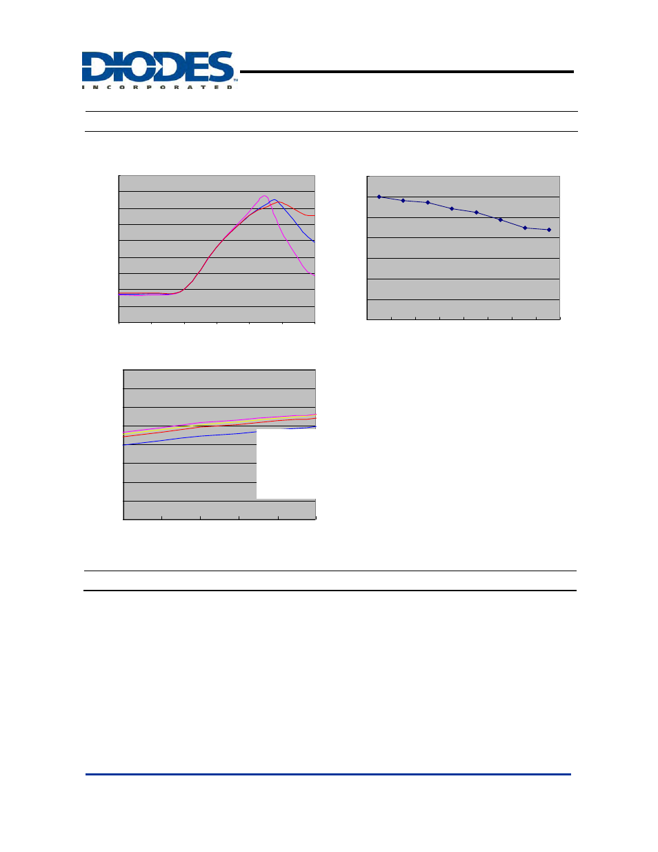
Typical Performance Characteristics
(Continued)
-90
-80
-70
-60
-50
-40
-30
-20
-10
0
1.0E+00
1.0E+01
1.0E+02
1.0E+03
1.0E+04
1.0E+05
1.0E+06
Power Supply Rejection Ratio
PS
RR
(
dB)
Frequency (Hz)
100mA
10mA
1mA
BP=0
0
0.1
0.2
0.3
0.4
0.5
0.6
0.7
1.5
1.8
2
2.5
2.8
3
3.3
3.5
Cur
re
n
t Lim
it
(A
)
Vout Vs Current Limit
Vcc=5V
Vout (V)
0
5 0
1 0 0
1 5 0
2 0 0
2 5 0
3 0 0
3 5 0
4 0 0
3 .5
4
4 .5
5
5 .5
6
V c c V s S h o r t C u r r e n t
V c c ( V )
S
h
ort
Curre
n
t (mA)
T o p t o b o t to m
V o u t= 1 .5 V
V o u t= 1 .8 V
V o u t= 2 .5 V
V o u t= 3 .3 V
Functional Description
The AP139 of CMOS regulators contain a PMOS pass transistor,
voltage reference, error amplifier, over-current protection,
thermal shutdown.
The P-channel pass transistor receives data from the error
amplifier, over-current protection, and thermal protection circuits.
During normal operation, the error amplifier compares the output
voltage to a precision reference. The over-current and thermal
shutdown circuits become active when the junction temperature
exceeds 130
o
C, or the current exceeds 300mA. During thermal
shutdown, the output voltage remains low. Normal operation is
restored when the junction temperature drops below 110
o
C.
The AP139 switches from voltage mode to current mode when
the load exceeds the rated output current. This prevents
over-stress.
Enable
The enable pin normally floats high. When actively, pulled low,
the PMOS pass transistor shuts off, and all internal circuits are
powered down. In this state, the quiescent current is less than
2
μA. This pin behaves much like an electronic switch.
External Capacitor
The AP139 is stable with a low ESR output capacitor to ground of
1.0
μF or greater. It can keep stable even with higher ESR
capacitors. A second capacitor is recommended between the
input and ground to stabilize V
IN
. The input capacitor should be
larger than 0.1
μF to have a beneficial effect. All capacitors should
be placed in close proximity to the pins. A “quiet” ground
termination is desirable.