Advance datasheet, Electrical characteristics, Parameter symbol test conditions min typ max unit – Diodes AP2821 User Manual
Page 6
Advance Datasheet
High-side Power Distribution Switch with Enable AP2821
Mar. 2013 Rev 2. 0 BCD Semiconductor Manufacturing Limited
6
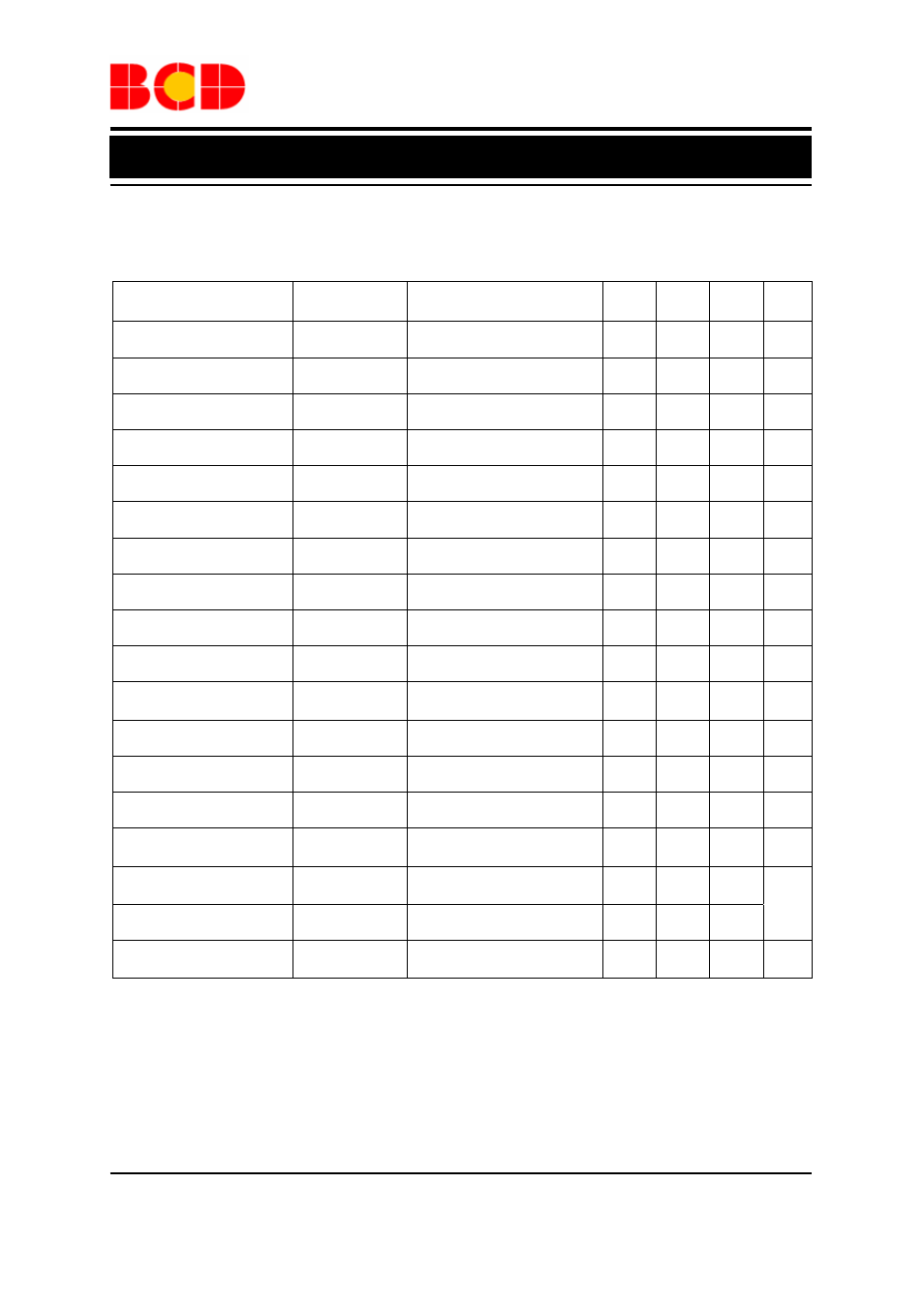
Electrical Characteristics
(V
IN
=5.0V, C
IN
=4.7
μF, C
OUT
=4.7
μF, Typical T
A
=25°C, unless otherwise specified)
Parameter Symbol
Test
Conditions
Min
Typ
Max
Unit
Input Voltage Range
V
IN
2.7 5.5
V
Switch On Resistance
R
DS(ON)
V
IN
=5V, I
OUT
=0.5A
120
140
m
Ω
Current Limit
I
LIMIT
V
OUT
=4.0V 1.5
2.0
2.8
A
Supply Current
I
SUPPLY
V
IN
=5V, R
LOAD
Open
35
65
μA
Fold-back Short Current
I
SHORT
V
OUT
=0V
1.5
A
Shutdown Supply Current
I
SHUTDOWN
V
EN
=0V, Shutdown Mode
0.1
1
μA
Output Leakage Current
I
LEAKAGE
V
EN
=0V, V
OUT
=0V
0.1
1
μA
Enable High Voltage
V
ENH
Enable Logic High
2.0
6.0
V
Enable Low Voltage
V
ENL
Enable Logic Low
0
1.2
V
Enable Pin Input Current
I
EN
Force 0V to 5.0V at EN Pin
0
1.0
μA
Under Voltage Lockout
Threshold Voltage
V
UVLO
V
IN
Increasing from 0V
2.2
2.5
2.7
V
Under Voltage Hysteresis
V
UVLOHY
0.2
V
Reverse Current
I
REVERSE
V
EN
=0V, V
OUT
>V
IN
0.1
1.0
μA
Shutdown Pull Low Resistance
R
DISCHARGE
V
EN
is disable
100
250
Ω
Output Turn-on Time
t
ON
From Enable Active to 90% of
Output, R
L
=10
Ω
1.9 ms
Thermal Shutdown
Temperature
T
OTSD
145
o
C
Thermal Shutdown Hysteresis
T
HYOTSD
20
Thermal Resistance
(Junction to Case)
θ
JC
70
ºC/W