Api9221, New prod uc t, Pin descriptions – Diodes API9221 User Manual
Page 2
API9221
CAR/WALL or USB SUPPLY INPUT LITHIUM BATTERY
CHARGER with OVP USB BYPASS and 10mA LDO
API9221
Document number: DS32204 Rev. 2 - 2
2 of 15
November 2011
© Diodes Incorporated
NEW PROD
UC
T
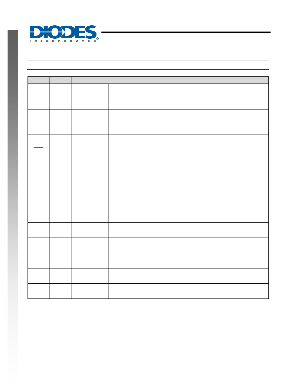
Pin Descriptions
Name
Pin #
Descriptions
VDC 1
Input pin from a
wall AC/DC or car
adapter
The recommended input to this pin is 4.5V to 6.7V with a maximum safe value of
28V. If a sufficient voltage is detected on VDC, no charge current is taken from
the VUSB pin. Internal OVP trips at 6.9V. The input current can be programmed
with a resistor at IVDC (pin 9). Decoupling with a 1
μF ceramic capacitor is
recommended.
VUSB 2
USB Host device
input
The recommended input to this pin is 4.5V to 5.3V with a maximum safe value of
28V. Internal OVP trips at 5.4V. The supply current drawn at this pin is the sum
of the charge current and the USB_BYP current. Decoupling with a 1
μF ceramic
capacitor is recommended. Special attention has to be given to the maximum
capacitance on the USB connection. Refer to the USB standard.
PPR
3
Power present
signal output,
active-low
The power present pin can indicate to a host processor that an external source is
present and that current can be derived from the input. This is an open drain
output pin, which goes LOW when a valid source voltage is connected to either
VUSB or VDC. If connected to a processor I/O a pull up resistor should be
utilized.
Alternatively this pin can be used to drive an indicator LED up to 10mA.
CHG
4
Charge indicator
output, active-low
Open drain pin is pulled LOW when charging is performed. Goes high when
charge current reaches IMIN. Remains high (including top-up), until the battery
voltage falls below 3.9V or the device is power cycled or
EN
is cycled. If
connected to a processor I/O a pull up resistor should be utilized.
Alternatively this pin can be used to drive an indicator LED up to 10mA.
EN
5
Charge enable
input, active-low
Logic level input pin to control charging from an external processor. An internal
600k
Ω (nominally) pull-down resistor is provided, This pin normally requires a
pull up resistor when connected to a processor I/O.
IMIN 6
Current setting for
end-of-charge
state
The end-of-charge current is set by a resistor connected from this pin to GND.
This applies to charging from either VDC or VUSB.
IUSB 7
Current setting,
USB Power
The USB input maximum charging current is set by a resistor connected from this
pin to GND. This current is also limited by a thermally controlled current fold-
back circuit.
GND
8
Ground
Ground return path.
IVDC 9
Current setting,
wall or car adapter
VDC input maximum charging current is set by a resistor connected from this pin
to GND. This current is also limited by a thermally controlled current fold-back
circuit.
USB_BYP 10
USB Bypass
output
Provides an external load path from the USB input, with current limiting. Protected
against reverse current.
BAT 11
Battery
connector
Connect this pin to the positive terminal of the battery. This pin is also used to
monitor the charge state of the battery. It is not recommended to operate the part
without a battery connected to this pin. Protected against reverse current.
VDC_LDO 12 LDO
output
Low current linear regulator for system supply, available when a valid VDC input
supply is used. Stabilize with a 0.1
μF to 1μF ceramic capacitor to ground.
Protected against reverse current.