Data sheet, Application information – Diodes AUR9719 User Manual
Page 14
Data Sheet
1.5MHz, 2A, STEP DOWN DC-DC CONVERTER AUR9719
Nov. 2011 Rev. 1. 0 BCD Semiconductor Manufacturing Limited
14
FB
GND
VOUT
R1
R2
AUR9719
Application Information
The basic AUR9719 application circuit is shown in
Figure 36, external components selection is determined
by the load current and is critical with the selection of
inductor and capacitor values.
1. Inductor Selection
For most applications, the value of inductor is chosen
based on the required ripple current with the range of
1
µH to 6.8µH.
The largest ripple current occurs at the highest input
voltage. Having a small ripple current reduces the ESR
loss in the output capacitor and improves the efficiency.
The highest efficiency is realized at low operating
frequency with small ripple current. However, larger
value inductors will be required. A reasonable starting
point for ripple current setting is △I
L
=40%I
MAX
. For a
maximum ripple current stays below a specified
value, the inductor should be chosen according to the
following equation:
The DC current rating of the inductor should be at
least equal to the maximum output current plus half
the highest ripple current to prevent inductor core
saturation. For better efficiency, a lower
DC-resistance inductor should be selected.
2. Capacitor Selection
The input capacitance, C
IN
, is needed to filter the
trapezoidal current at the source of the top MOSFET.
To prevent large ripple voltage, a low ESR input
capacitor sized for the maximum RMS current must
be used. The maximum RMS capacitor current is
given by:
It indicates a maximum value at V
IN
=2V
OUT
, where
I
RMS
=I
OUT
/2. This simple worse-case condition is
commonly used for design because even significant
deviations do not much relieve. The selection of C
OUT
is determined by the Effective Series Resistance
(ESR) that is required to minimize output voltage
ripple and load step transients, as well as the amount
of bulk capacitor that is necessary to ensure that the
control loop is stable. Loop stability can be also
checked by viewing the load step transient response
as described in the following section. The output
ripple, △V
OUT
, is determined by:
The output ripple is the highest at the maximum input
voltage since △I
L
increases with input voltage.
3. Load Transient
A switching regulator typically takes several cycles to
respond to the load current step. When a load step
occurs, V
OUT
immediately shifts by an amount equal
to △I
LOAD
×
ESR, where ESR is the effective series
resistance of output capacitor. △I
LOAD
also begins to
charge or discharge C
OUT
generating a feedback error
signal used by the regulator to return V
OUT
to its
steady-state value. During the recovery time, V
OUT
can be monitored for overshoot or ringing that would
indicate a stability problem.
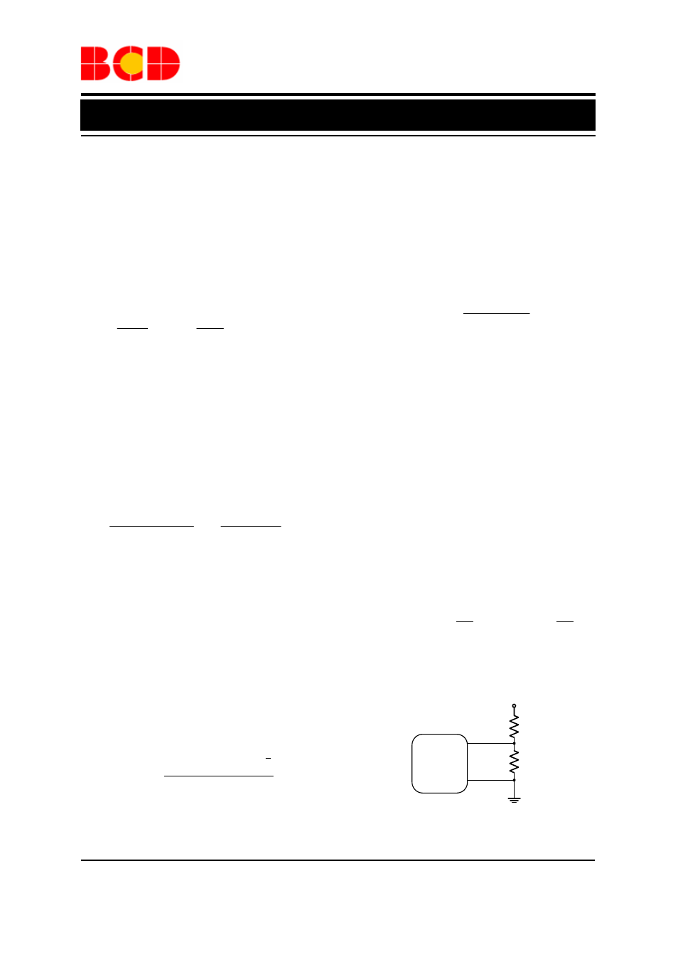
4. Output Voltage Setting
The output voltage of AUR9719 can be adjusted by a
resistive divider according to the following formula:
The resistive divider senses the fraction of the output
voltage as shown in Figure 34.
Figure 34. Setting the Output Voltage
IN
OUT
IN
OUT
OMAX
RMS
V
V
V
V
I
I
2
1
)]
(
[
−
×
=
)
1
(
1
IN
OUT
OUT
L
V
V
V
L
f
I
−
×
=
∆
]
)
(
1
][
)
(
[
MAX
V
V
MAX
I
f
V
L
IN
OUT
L
OUT
−
∆
×
=
]
8
1
[
OUT
L
OUT
C
f
ESR
I
V
Ч
Ч
+
∆
≤
∆
)
1
(
8
.
0
)
1
(
2
1
2
1
R
R
V
R
R
V
V
REF
OUT
+
Ч
=
+
Ч
=