Pin descriptions, Functional block diagram – Diodes AP65400 User Manual
Page 2
AP65400
Document number: DS36497 Rev. 1 - 2
2 of 15
www.diodes.com
April 2014
© Diodes Incorporated
AP65400
Pin Descriptions
Pin
Name
Pin Number
Function
BS 1
High-Side Gate Drive Boost Input. BS supplies the drive for the high-side N-Channel MOSFET a
0.01µF or greater capacitor from SW to BS to power the high side switch.
IN 2
Power Input. IN supplies the power to the IC, as well as the step-down converter switches. Drive IN
with a 4.75V to 18V power source. Bypass IN to GND with a suitably large capacitor to eliminate noise
on the input to the IC. See Input Capacitor.
SW 3
Power Switching Output. SW is the switching node that supplies power to the output. Connect the
output LC filter from SW to the output load. Note that a capacitor is required from SW to BS to power
the high-side switch.
GND 4
Ground
FB 5
Feedback Input. FB senses the output voltage and regulates it. Drive FB with a resistive voltage
divider connected to it from the output voltage. The feedback threshold is 0.800V. See Setting the
Output Voltage.
COMP 6
Compensation Node. COMP is used to compensate the regulation control loop. Connect a series RC
network from COMP to GND. In some cases, an additional capacitor from COMP to GND is required.
See Compensation Components.
EN 7
Enable Input. EN is a digital input that turns the regulator on or off. Drive EN high to turn on the
regulator; low to turn it off. Attach to IN with a 100kΩ pull up resistor for automatic startup.
SS 8
Soft-Start Control Input. SS controls the soft-start period. Connect a capacitor from SS to GND to set
the soft-start period. A 0.1µF capacitor sets the soft-start period to 13ms. To disable the soft-start
feature, leave SS floating.
EP
EP
Exposed Pad is connected to ground
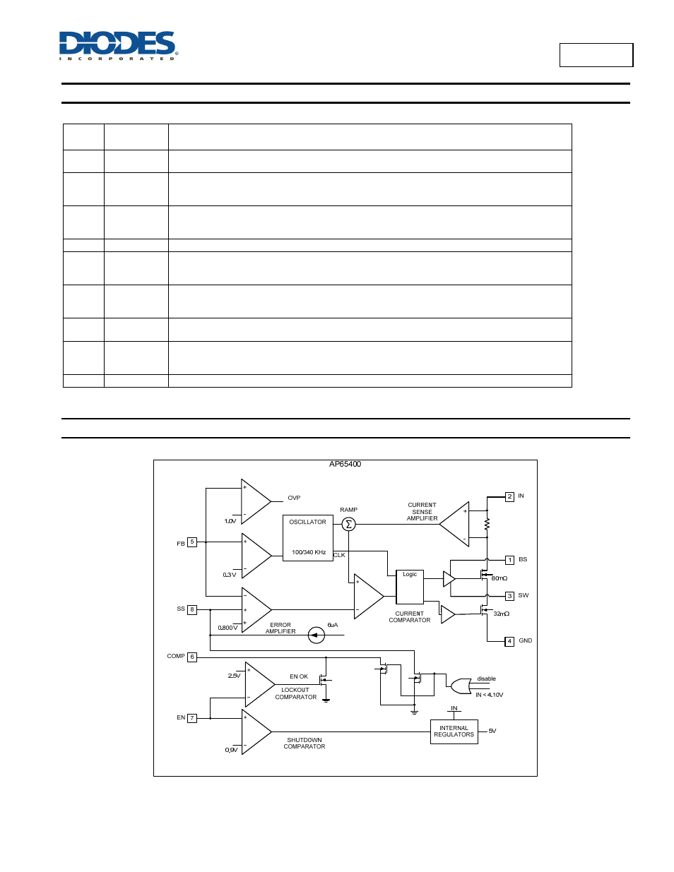
Functional Block Diagram
Figure 2. Functional Block Diagram