New prod uc t ap6503a, Application information – Diodes AP6503A User Manual
Page 9
AP6503A
Document number: DS36000 Rev. 2 - 2
9 of 15
December 2012
© Diodes Incorporated
NEW PROD
UC
T
AP6503A
Application Information
(cont.)
Under Voltage Lockout (UVLO)
Under Voltage Lockout is implemented to prevent the IC from insufficient input voltages. The AP6503A has a UVLO comparator that monitors
the input voltage and the internal bandgap reference. If the input voltage falls below 4.0V, the AP6503A will latch an under voltage fault. In this
event the output will be pulled low and power has to be re-cycled to reset the UVLO fault.
Over Voltage Protection
When the AP6503A FB pin exceeds 20% of the nominal regulation voltage of 0.925V, the over voltage comparator is tripped and the COMP pin
and the SS pin are discharged to GND, forcing the high-side switch off.
Thermal Shutdown
The AP6503A has on-chip thermal protection that prevents damage to the IC when the die temperature exceeds safe margins. It implements a
thermal sensing to monitor the operating junction temperature of the IC. Once the die temperature rises to approximately 160°C, the thermal
protection feature gets activated. The internal thermal sense circuitry turns the IC off thus preventing the power switch from damage.
A hysteresis in the thermal sense circuit allows the device to cool down to approximately +120°C before the IC is enabled again through soft
start. This thermal hysteresis feature prevents undesirable oscillations of the thermal protection circuit.
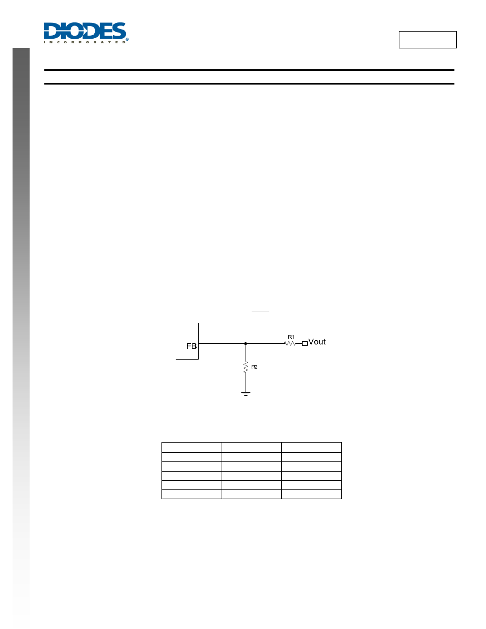
Setting the Output Voltage
The output voltage can be adjusted from 0.925V to 18V using an external resistor divider. Table 1 shows a list of resistor selection for common
output voltages. Resistor R1 is selected based on a design tradeoff between efficiency and output voltage accuracy. For high values of R1 there
is less current consumption in the feedback network. However the trade off is output voltage accuracy due to the bias current in the error
amplifier. R1 can be determined by the following equation:
⎟⎟
⎠
⎞
⎜⎜
⎝
⎛
−
⋅
=
1
0.925
V
R
R
OUT
2
1
Figure 4. Feedback Divider Network
When output voltage is low, network as shown in
Figure 4 is recommended.
V
OUT
(V)
R1(K
Ω) R2(KΩ)
5 45.3 10
3.3 26.1 10
2.5 16.9 10
1.8 9.53 10
1.2 3 10
Table 1. Resistor Selection for Common Output Voltages