Preliminary datasheet, Pin configuration, Pin description – Diodes AP3421/A/B User Manual
Page 2: Pin number pin name function
Preliminary Datasheet
1.3MHz, Dual 1.0A Synchronous Step-down Converters AP3421/A/B
Feb. 2013 Rev. 1. 4 BCD Semiconductor Manufacturing Limited
2
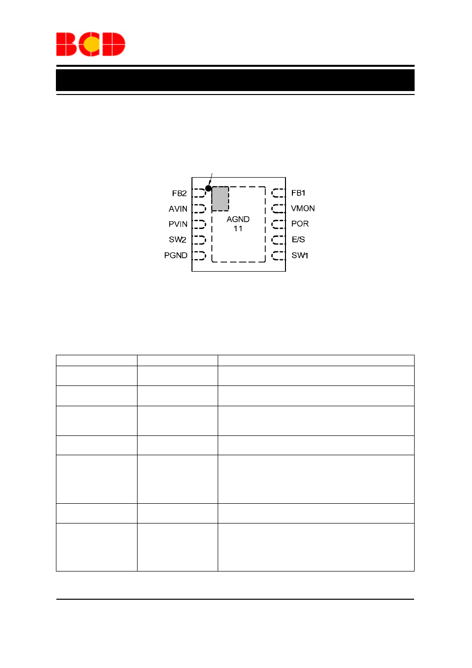
Pin Configuration
DN Package
(DFN-3×3-10)
Pin 1 Mark
1
2
3
4
5
6
7
8
9
10
Figure 2. Pin Configuration of AP3421/A/B (Top View)
Pin Description
Pin Number
Pin Name
Function
1 FB2
Feedback from VO2. Connect voltage divider to the
load side of VO2 output inductor-capacitor filter
2 AVIN
Analog power input. Connect a 1
µF ceramic capacitor
between this pin and AGND
3 PVIN
Control MOSFET switch power input. Connect a 10
µF
ceramic capacitor between this pin and PGND, as close
to the IC as possible
4 SW2
VO2 synchronous buck switching output. Connect to
VO2 inductor
5 PGND
Power ground connection. Synchronous rectifier
MOSFET source. Provide a star connection between
this pin, VO1, VO2 filter capacitor returns, VIN input
capacitor return, and AGND. Keep the star connection
as close to the IC as possible
6 SW1
VO1 synchronous buck switching output. Connect to
VO1 inductor
7 E/S
Enable/Synchronization. Pulling this pin high statically
enables the IC and pulling the pin low statically will
shut down the IC. Applying a pulse to this pin will
synchronize SW1 and SW2 switching frequency to ½
the external clock frequency