Preliminary datasheet, Pin configuration, Pin description – Diodes AP3422 User Manual
Page 2

Preliminary Datasheet
Dual 1.1MHz, 800mA Synchronous DC-DC Buck Converter AP3422
Feb. 2013 Rev. 1. 2 BCD Semiconductor Manufacturing Limited
2
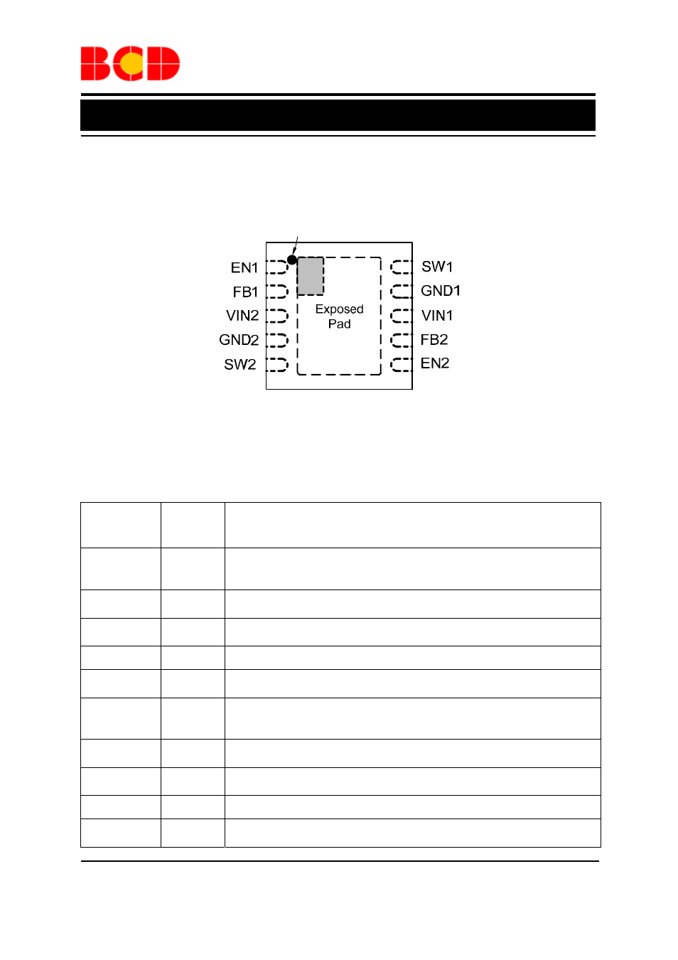
Pin Configuration
DN Package
(DFN-3×3-10)
Pin 1 Mark
1
2
3
4
5
6
7
8
9
10
Figure 2. Pin Configuration of AP3422 (Top View)
Pin Description
Pin Number
Pin Name
Function
1 EN1
Channel 1 enable control input. Drive EN1 above 1.5V to turn on the
Channel 1. Drive EN1 below 0.6V to turn it off (shutdown current <
0.1µA)
2 FB1
Channel 1 feedback input. Connect FB1 to the center point of the external
resistor divider. The feedback voltage is 0.6V
3 VIN2
Channel 2 supply input. Bypass to GND with a 10µF or greater ceramic
capacitor
4 GND2
Ground
2
5 SW2
Channel 2 power switch output. Inductor connection to drains of the
internal PFET and NFET switches
6 EN2
Channel 2 Enable Control Input. Drive EN2 above 1.5V to turn on the
Channel 2. Drive EN2 below 0.6V to turn it off (shutdown current <
0.1µA)
7 FB2
Channel 2 feedback input. Connect FB2 to the center point of the external
resistor divider. The feedback voltage is 0.6V
8 VIN1
Channel 1 supply input. Bypass to GND with a 10µF or greater ceramic
capacitor
9 GND1
Ground
1
10 SW1
Channel 1 power switch output. Inductor connection to drains of the
internal PFET and NFET switches
