Ap3418, Pin descriptions, Functional block diagram – Diodes AP3418 User Manual
Page 2

AP3418
Document number: DS37233 Rev.
2 - 2
2 of 11
April 2014
© Diodes Incorporated
AP3418
A Product Line of
Diodes Incorporated
Pin Descriptions
Pin Number
Pin Name
Function
1
EN
Control input pin. Forcing this pin above 1.5V enables the IC. Forcing this
pin below 0.4V shuts down the IC. When the IC is in shutdown mode, all
functions are disabled to decrease the supply current below 1µA
2
GND
Ground pin
3
SW
Power switch output pin. Inductor connection to drain of the internal PFET
and NFET switches
4
VIN
Supply input pin. Bypass to GND with a 4.7µF or greater ceramic
capacitor
5
FB
This is the feedback pin of the device. Connect this pin directly to the
output if the fixed output voltage version is used. For the adjustable
version, an external resistor divider is connected to this pin
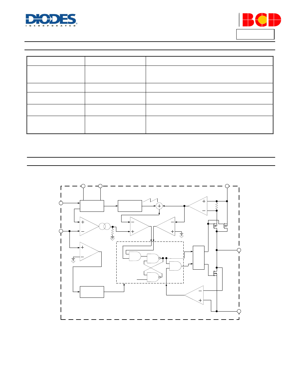
Functional Block Diagram
VOLTAGE
REFERENCE
OSCILLATOR
CURRENT
SENSE
ERROR
AMPLIFIER
PWM
COMPARATOR
MAX
CURRENT LIMIT
0.6V
V
OCP
0.4V
LOGIC
CLK
D
R
IV
E
R
SHORT
CIRCUIT
PROTECTION
REVERSE
COMPARATOR
EN
FB
GND
SW
GND
VIN
VIN
1
5
2
4
3
4
2
