Data sheet, Pin configuration, Pin description – Diodes AP3406A User Manual
Page 2
Data Sheet
1.1MHz, 800mA SYNCHRONOUS DC-DC BUCK CONVERTER AP3406A
Feb. 2013 Rev. 1. 5 BCD Semiconductor Manufacturing Limited
2
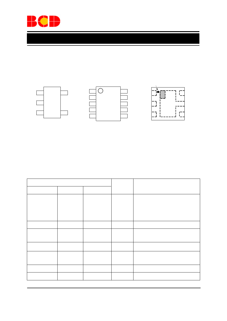
Pin Configuration
KT Package MM Package DN Package
TSOT-23-5 MSOP-10 DFN-2×2-6(1)
Figure 2. Pin Configuration of AP3406A (Top View)
Pin Description
Pin Number
Pin Name
Function
TSOT-23-5 MSOP-10
DFN-2×2-6(1)
1 8 2
EN
Control input pin. Forcing this pin above
1.5V enables the IC. Forcing this pin
below 0.6V shuts down the IC. When
the IC is in shutdown mode, all
functions are disabled to decrease the
supply current below 1
µA
2 3 5
GND
Ground
pin
3 9 4
SW
Power switch output pin. Inductor
connection to drain of the internal PFET
and NFET switches
4 1 3
VIN
Supply input pin. Bypass to GND with a
10
µF or greater ceramic capacitor
5 5 6
FB
Feedback pin. Connect it with an
external resistor divider network to
program the system output voltage
2, 4, 6, 7
1
NC
No connection
10
PGND
Power ground pin
NC
EN
VIN
FB
GND
SW
P in 1 Mark
1
2
3
4
5
6
EN
SW
GND
VIN
FB
1
2
3
4
5
1
2
3
4
8
7
5
6
9
10
EN
VIN
NC
GND
NC
FB
NC
NC
SW
PGND