Preliminary datasheet, Pin configuration, Pin description – Diodes AP3201A User Manual
Page 2
Preliminary Datasheet
380kHz, 2A Asynchronous DC-DC Buck Converter AP3201A
Mar. 2011 Rev. 1. 0 BCD Semiconductor Manufacturing Limited
2
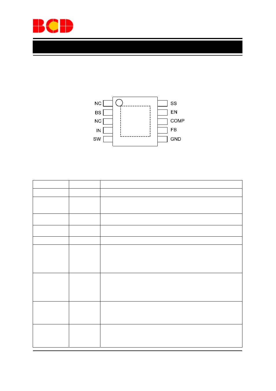
Pin Configuration
MH Package
(HMSOP-10)
1
2
3
4
8
7
5
6
9
10
Figure 2. Pin Configuration of AP3201A (Top View)
Pin Description
Pin Number
Pin Name
Function
1, 3
NC
No connection or tied to ground
2
BS
Bootstrap pin. A bootstrap capacitor is connected between the BS pin
and SW pin. The voltage across the bootstrap capacitor drives the
internal high-side power MOSFET
4
IN
Supply input pin. A capacitor should be connected between the IN pin
and GND pin to keep the input voltage constant
5
SW
Power switch output pin. This pin is connected to the inductor and
bootstrap capacitor
6
GND Ground
pin
7
FB
Feedback pin. This pin is connected to an external resistor divider to
program the system output voltage. When the FB pin voltage exceeds
20% of the nominal regulation value of 0.920V, the over voltage
protection is triggered. When the FB pin voltage is below 0.6V, the
oscillator frequency is lowered to realize short circuit protection
8
COMP
Compensation pin. This pin is the output of the transconductance
error amplifier and the input to the current comparator. It is used to
compensate the control loop. Connect a series RC network from this
pin to GND. In some cases, an additional capacitor from this pin to
GND pin is required
9
EN
Control input pin. Forcing this pin above 1.5V or set this pin floating
enables the IC. Forcing this pin below 0.5V shuts down the IC. When
the IC is in shutdown mode, all functions are disabled to decrease the
supply current below 1
µA
10
SS
Soft-start control input pin. SS controls the soft start period. Connect
a capacitor from SS to GND to set the soft-start period. A 0.1
µF
capacitor sets the soft-start period to 10ms. To disable the soft-start
feature, leave SS unconnected