Micro power step-up dc-dc converter ap3015/a, Data sheet, Typical performance characteristics (continued) – Diodes AP3015/A User Manual
Page 8: Application information, Operating principles
MICRO POWER STEP-UP DC-DC CONVERTER AP3015/A
8
May 2010 Rev. 1. 4
BCD Semiconductor Manufacturing Limited
Data Sheet
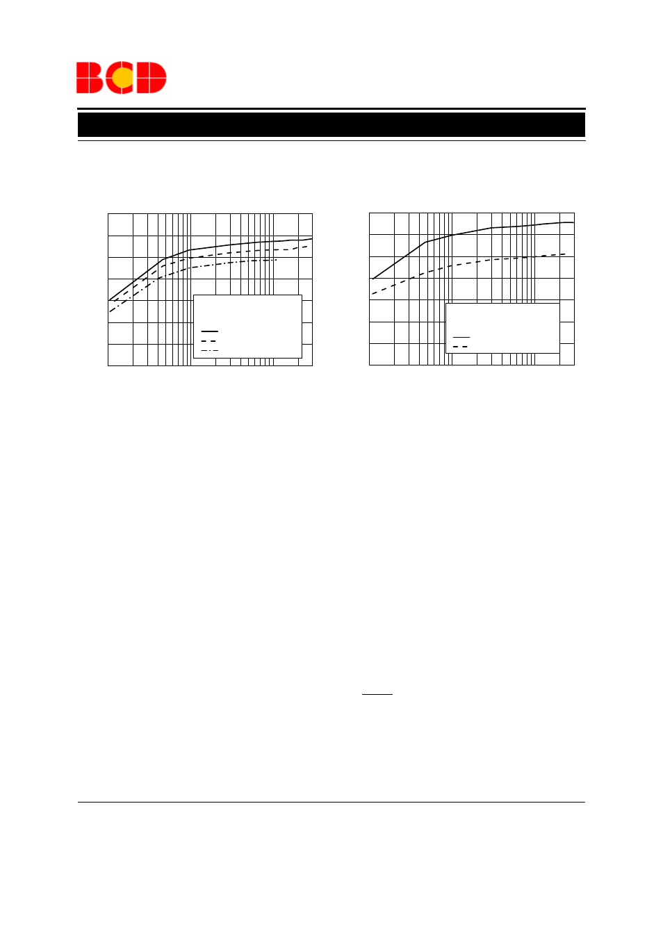
Figure 13. Efficiency
Typical Performance Characteristics (Continued)
Figure 12. Efficiency
Unless otherwise noted, V
IN
=1.2V
Application Information
Operating Principles
AP3015/A feature a constant off-time control scheme.
Refer to Figure 3, the bandgap voltage V
REF
(1.23V
typical) is used to control the output voltage.
When the voltage at the FB pin drops below the lower
hysteresis point of Feedback Comparator (typical
hysteresis is 8mV), the Feedback Comparator enables
the chip and the NPN power switch is turned on, the
current in the inductor begins to ramp up and store
energy in the coil while the load current is supplied by
the output capacitor. Once the current in the inductor
reaches the current limit, the Current-Limit
Comparator resets the 400ns One-Shot which turns off
the NPN switch for 400ns. The SW voltage rises to the
output voltage plus a diode drop and the inductor
current begins to ramp down. During this time the
energy stored in the inductor is transferred to C
OUT
and the load. After the 400ns off-time, the NPN switch
is turned on and energy will be stored in the inductor
again.
This cycle will continue until the voltage at FB pin
reaches 1.23V, the Feedback Comparator disables the
chip and turns off the NPN switch. The load current is
then supplied solely by output capacitor and the output
voltage will decrease. When the FB pin voltage drops
below the lower hysteresis point of Feedback
Comparator, the Feedback Comparator enables the
device and repeats the cycle described previously.
Under not switching condition, the I
Q
of the device is
about 17
µA.
The AP3015/A contain additional circuitry to provide
protection during start-up or under short-circuit
conditions. When the FB pin voltage is lower than
approximately 0.6V, the switch off-time is increased
to 1.5
µs and the current limit is reduced to about
250mA (70mA for AP3015A). This reduces the
average inductor current and helps to minimize the
power dissipation in the AP3015/A power switch, in
the external inductor and in the diode.
The SHDN pin can be used to turn off the AP3015/A
and reduce the I
Q
to less than 1
µA. In shutdown mode
the output voltage will be a diode drop below the input
voltage.
0.1
1
10
50
55
60
65
70
75
80
85
E
ffi
ci
en
cy
(
%
)
Load Current (mA)
AP3015
V
OUT
=20V, L=10
µ
H, C
OUT
=1
µ
F
Refer to Figure 14
V
IN
=4.2V
V
IN
=3.3V
V
IN
=2.5V
0.1
1
10
50
55
60
65
70
75
80
85
E
ffi
ci
en
cy
(
%
)
Load Current (mA)
AP3015A
V
OUT
=3.3V, L=10
µ
H, C
OUT
=20
µ
F
Refer to Figure 15
V
IN
=2.5V
V
IN
=1.2V