Electrical characteristics – Diodes AZ34063C User Manual
Page 5
1A STEP-DOWN/STEP-UP/INVERTING DC-DC CONVERTER AZ34063C
Data Sheet
5
Jan. 2013 Rev. 1. 7
BCD Semiconductor Manufacturing Limited
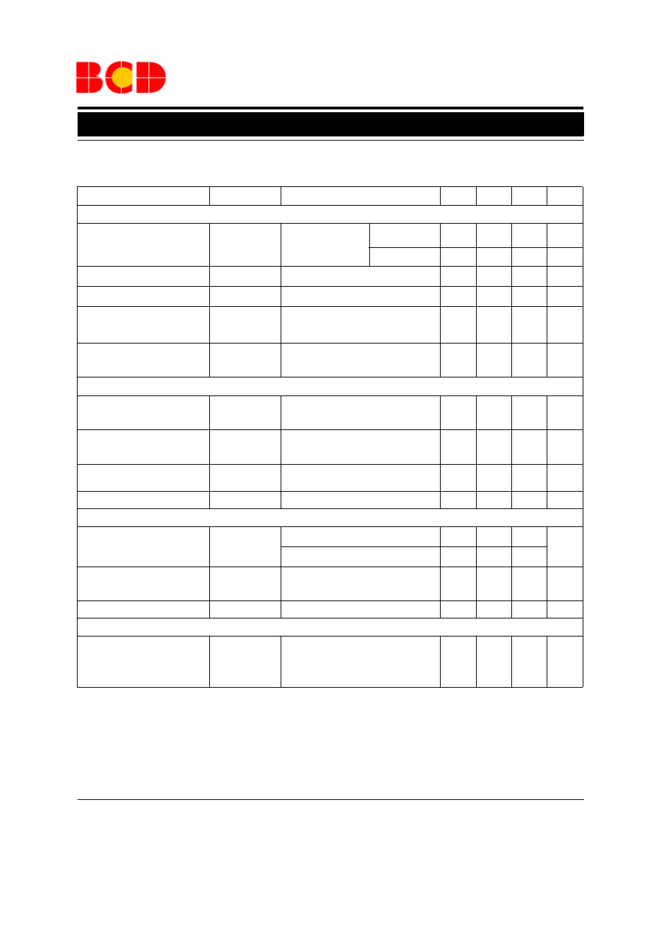
(
V
CC
=5.0 V, T
A
=-40 to 85
o
C, unless otherwise specified.)
Note 3: Low duty cycle pulse technique are used during test to maintain junction temperature as close to ambient temperature
as possible.
Note 4: If the output switch is driven into hard saturation (non-Darlington configuration) at low switch currents (
≤ 300mA) and
high driver currents (
≥ 30mA), it may take up to 2.0us for it to come out of saturation. This condition will shorten the off time
at frequencies 30KHz, and is magnified at high temperatures. This condition does not occur with a Darlington configuration,
since the output switch cannot saturate. If a non-Darlington configuration is used, the following output drive condition is rec-
ommended:
Parameter
Symbol
Conditions
Min
Typ
Max
Unit
OSCILLATOR
Frequency
f
OSC
V
PIN5
=0V,
T
A
=25
o
C
C
T
=1.0nF
30
38
45
KHz
C
T
=330pF
75
88
100
KHz
Charge Current
I
CHG
V
CC
=5.0V to 36 V, T
A
=25
o
C
30
38
45
μA
Discharge Current
I
DISCHG
V
CC
=5.0V to 36V, T
A
=25
o
C
180
240
290
μA
Discharge to Charge
Current Ratio
I
DISCHG
/I
CHG
Pin 7 to V
CC
, T
A
=25
o
C
5.2
6.5
7.5
Current Limit Sense
Voltage
V
IPK
(sense) I
CHG
=I
DISCHG
, T
A
=25
o
C
250
300
350
mV
OUTPUT SWITCH (Note 3)
Saturation Voltage,
Dalington Connection
V
CE
(sat)
I
SW
=1A, Pins 1, 8 connected,
Common Emitter
1.0
1.3
V
Saturation Voltage (Note 4)
V
CE
(sat)
I
SW
=1A, R
PIN8
=82
Ω to V
CC
,
Forced
β=20, Common Emitter
0.45
0.8
V
DC Current Gain
h
FE
I
SW
=1A, V
CE
=5.0V, T
A
=25
o
C
50
75
Collector Off-State Current
I
C
(off)
V
CE
=36V
0.01
100
μA
COMPARATOR
Threshold Voltage
V
TH
T
A
=25
o
C
1.225 1.250 1.275
V
T
A
=-40 to 85
o
C
1.21
1.250
1.29
Threshold Voltage Line
Regulation
R
EGLINE
V
CC
=3.0V to 36V
1.4
5
mV
Input Bias Current
I
IB
V
IN
=0V
-20
-400
nA
TOTAL DEVICE
Supply Current
I
CC
V
CC
=5.0V to 36V, C
T
=1.0 nF,
V
PIN7
=V
CC
, V
PIN5
> V
TH
,
V
PIN2
=GND, other pins open
4
mA
Electrical Characteristics