Package thermal data, Recommended operating conditions, Electrical characteristics – npn transistor – q1 – Diodes AL5802 User Manual
Page 3
AL5802
Document number: DS35516 Rev. 9 - 2
3 of 11
March 2014
© Diodes Incorporated
ADVAN
CE I
N
F
O
RM
ATI
O
N
NEW PROD
UC
T
AL5802
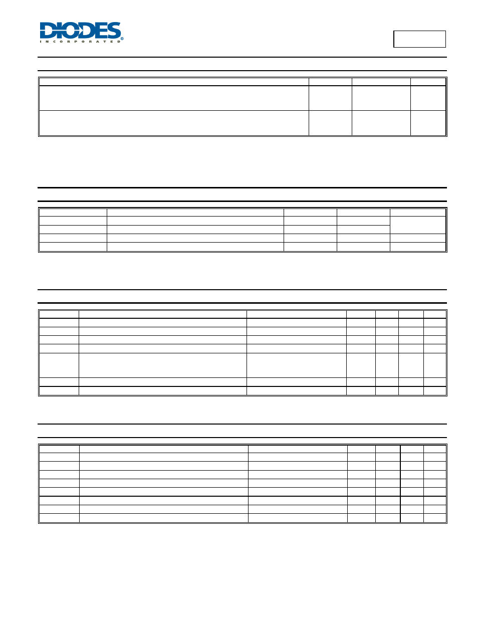
Package Thermal Data
Characteristic Symbol
Value
Unit
Power Dissipation (Note 5) @ T
A
= +25°C
Power Dissipation (Note 6) @ T
A
= +25°C
Power Dissipation (Note 7) @ T
A
= +25°C
P
D
0.37
0.87
1
W
Thermal Resistance, Junction to Ambient Air (Note 5) @ T
A
= +25°C
Thermal Resistance, Junction to Ambient Air (Note 6) @ T
A
= +25°C
Thermal Resistance, Junction to Ambient Air (Note 7) @ T
A
= +25°C
R
θJA
335
143
120
°C/W
Notes:
5. Device mounted on FR-4 PCB, 2oz with minimum recommended pad layout.
6. Device mounted on 25mm x 25mm 2oz copper board.
7. Device mounted on 50mm x 50mm 2oz copper board.
Recommended Operating Conditions
Symbol Parameter Min
Max
Unit
V
BIAS
Supply voltage range
4.5
30
V
V
OUT
OUT voltage range
0.8
30
I
LED
LED pin current (Note 8)
10
120
mA
T
A
Operating ambient temperature range
-40
+125
°C
Note:
8. Subject to ambient temperature, power dissipation and PCB.
Electrical Characteristics – NPN Transistor – Q1
(@T
A
= +25°C, unless otherwise specified.)
Symbol Characteristic
Test
Condition
Min
Typ
Max
Unit
V
(BR)CEO
Collector-Emitter Breakdown Voltage (Note 9)
I
C
= 1.0mA, I
B
= 0
40 — — V
V
(BR)EBO
Emitter-Base Breakdown Voltage
I
E
= 10µA, I
C
= 0
6.0 — — V
I
CEX
Collector Cutoff Current
V
CE
= 30V, V
EB(OFF)
= 3.0V
— — 50 nA
I
BL
Base Cutoff Current
V
CE
= 30V, V
EB(OFF)
= 3.0V
— — 50 nA
h
FE
DC Current Gain
I
C
= 100µA, V
CE
= 1.0V
I
C
= 1.0mA, V
CE
= 1.0V
I
C
= 10mA, V
CE
= 1.0V
40
70
100
—
—
—
—
—
300
—
V
CE(SAT)
Collector-Emitter Saturation Voltage (Note 9)
I
C
= 10mA, I
B
= 1.0mA
— —
0.20
V
V
BE(SAT)
Base-Emitter Saturation Voltage
I
C
= 10mA, I
B
= 1.0mA
0.65 — 0.85 V
Electrical Characteristics – NPN Pre-biased Transistor – Q2
(@T
A
= +25°C, unless otherwise specified.)
Symbol Characteristic
Test
Condition
Min
Typ
Max
Unit
V
(BR)CBO
Collector-Base Breakdown Voltage
I
C
= 50μA, I
E
= 0
30 — — V
V
(BR)CEO
Collector-Emitter Breakdown Voltage (Note 9)
I
C
= 1mA, I
B
= 0
30 — — V
V
(BR)EBO
Emitter-Base Breakdown Voltage
I
E
= 50μA, I
C
= 0
5.0 — — V
I
CBO
Collector Cut-Off Current
V
CB
= 30V, I
E
= 0
— —
0.5
µA
I
EBO
Emitter Cut-Off Current
V
EB
= 4V, I
C
= 0
— —
0.5
µA
V
CE(SAT)
Collector-Emitter Saturation Voltage (Note 9)
I
C
= 10mA, I
B
= 1mA
— —
0.3 V
h
FE
DC Current Gain (Note 9)
V
CE
= 5V, I
C
= 150mA
100 — — —
R
1
Input Resistance
—
7
10
13
kΩ
*Characteristics of transistor only.
Note:
9. Short duration pulse test used to minimize self-heating effect.