Maximum ratings, Thermal characteristics, Electrical characteristics – Diodes D5V0L1B2S9 User Manual
Page 2
D5V0L1B2S9
Document number: DS36458 Rev. 6 - 2
2 of 5
March 2014
© Diodes Incorporated
D5V0L1B2S9
NEW PROD
UC
T
Maximum Ratings
(@T
A
= +25°C, unless otherwise specified.)
Characteristic Symbol
Value
Unit
Conditions
Peak Pulse Power Dissipation
P
PP
84 W
8/20μs, per Figure 1
Peak Pulse Current
I
PP
6 A
8/20μs, per Figure 1
ESD Protection – Contact Discharge
V
ESD_Contact
±30
kV
IEC 61000-4-2 Standard
ESD Protection – Air Discharge
V
ESD_Air
±30
kV
IEC 61000-4-2 Standard
Thermal Characteristics
Characteristic Symbol
Value
Unit
Package Power Dissipation (Note 5)
P
D
250 mW
Thermal Resistance, Junction to Ambient (Note 5)
R
θJA
500 °C/W
Operating and Storage Temperature Range
T
J
, T
STG
-65 to +150
°C
Electrical Characteristics
(@T
A
= +25°C, unless otherwise specified.)
Characteristic
Symbol
Min
Typ
Max
Unit
Test Conditions
Reverse Standoff Voltage
V
RWM
— — 5 V
—
Channel Leakage Current (Note 6)
I
RM
—
10 100 nA
V
RWM
= 5V
Clamping Voltage, Positive Transients
V
CL
—
7.0 9.0
V
I
PP
= 1A, t
p
= 8/20μS
— 8.7 10.7
I
PP
= 3A, t
p
= 8/20μS
—
10.5 12.0
I
PP
= 5A, t
p
= 8/20μS
—
11.5 14.0
I
PP
= 6A, t
p
= 8/20μS
Breakdown Voltage
V
BR
6 7 8 V
I
R
= 1mA
Differential Resistance
R
DIF
—
0.2 — Ω
I
R
= 1A, t
p
= 8/20μS
Channel Input Capacitance
C
IN
—
15 20 pF
V
R
= 0V, f = 1MHz
Notes:
5. Device mounted on FR-4 PCB pad layout (2oz copper) as shown on Diodes, Inc. suggested pad layout AP02001, which can be found on our website at
6. Short duration pulse test used to minimize self-heating effect.
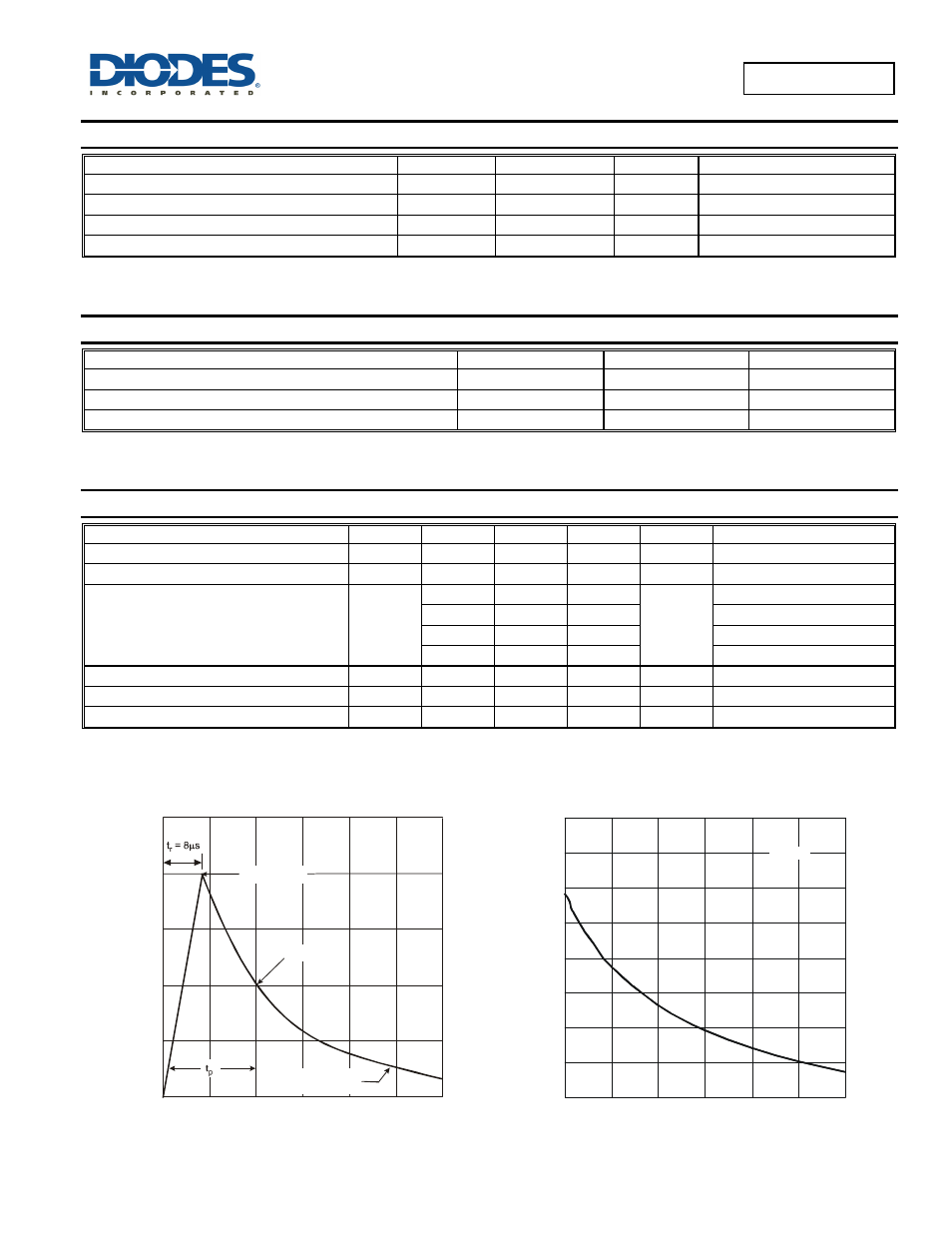
0
t, TIME (µs)
Figure 1 Pulse Waveform
20
40
60
100
50
0
Peak Value I
pp
Half Value I /2
pp
8x20 Waveform
as defined by R.E.A.
I
, PEA
K PUL
SE
CURREN
T
(
%
I
)
Pp
p
P
10
11
12
13
14
15
16
17
18
0
1
2
3
4
5
6
V , REVERSE VOLTAGE (V)
Figure 2 Typical Total Capacitance vs. Reverse Voltage
R
C
, T
O
TAL
C
A
P
A
C
IT
A
N
C
E (
p
F)
T
f = 1MHz