Thermal characteristics, Electrical characteristics – Diodes D18V0L1B2LP User Manual
Page 2
D18V0L1B2LP
Document number: DS36461 Rev. 1 - 2
2 of 5
March 2014
© Diodes Incorporated
D18V0L1B2LP
NEW PROD
UC
T
Thermal Characteristics
Characteristic Symbol
Value
Unit
Package Power Dissipation (Note 5)
P
D
250 mW
Thermal Resistance, Junction to Ambient (Note 5)
R
θJA
500
°C/W
Operating and Storage Temperature Range
T
J
, T
STG
-65 to +150
°C
Electrical Characteristics
(@T
A
= +25°C, unless otherwise specified.)
Characteristic
Symbol
Min
Typ
Max
Unit
Test Conditions
Reverse Standoff Voltage
V
RWM
—
— 18 V
—
Channel Leakage Current (Note 6)
I
RM
— — 100 nA
V
RWM
= 18V
Clamping Voltage, Positive Transients
V
CL
—
27
30 V
I
PP
= 1A, t
p
= 8/20μS
— 30 34 V
I
PP
= 2A, t
p
= 8/20μS
Breakdown Voltage
V
BR
21
—
25 V
I
R
= 1mA
Differential Resistance
R
DIF
—
2.2 — Ω
I
R
= 1A, t
p
= 8/20μS
Channel Input Capacitance
C
T
—
7.0 12 pF
V
R
= 0V, f = 1MHz
Notes:
5. Device mounted on FR-4 PCB pad layout (2oz copper) as shown on Diodes, Inc. suggested pad layout AP02001, which can be found on our website at
6. Short duration pulse test used to minimize self-heating effect.
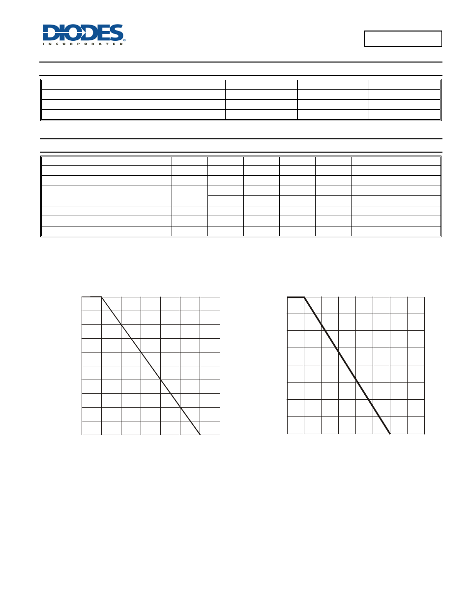
0
125
175
150
50
100
0
T , AMBIENT TEMPERATURE ( C)
Figure 1 Power Derating Curve
A
°
P
, P
O
WE
R
D
IS
S
IP
A
T
IO
N
(mW
)
D
25
100
50
75
150
25
75
125
250
175
Note 5
200
225
0
50
25
50
75
100 125
150
P
EAK
P
U
LS
E
D
E
R
A
T
IN
G
%
O
F
P
EAK
POW
E
R OR
CUR
RENT
T , AMBIENT TEMPERATURE (°C)
Figure 2 Pulse Derating Curve
A
0
100
25
75
175 200