Thermal characteristics, Electrical characteristics – Diodes D12V0H1U2WS User Manual
Page 2
D12V0H1U2WS
Document number: DS36723 Rev. 1 - 2
2 of 4
January 2014
© Diodes Incorporated
D12V0H1U2WS
NEW PROD
UC
T
Thermal Characteristics
Characteristic Symbol
Value
Unit
Package Power Dissipation (Note 5)
P
D
200 mW
Thermal Resistance, Junction to Ambient (Note 5)
R
θJA
625
°C/W
Operating Temperature Range
T
J
-55 to +125
°C
Storage Temperature Range
T
STG
-65 to +150
°C
Electrical Characteristics
(@T
A
= +25°C, unless otherwise specified.)
Characteristic Symbol
Min
Typ
Max
Unit
Test
Conditions
Reverse Working Voltage
V
RWM
—
—
12.0
V
—
Reverse Current (Note 6)
I
R
— 10 100
nA
V
R
= V
RWM
= 12.0V
Reverse Breakdown Voltage
V
BR
13.3 —
15.75 V
I
R
= 1mA
Reverse Clamping Voltage
V
CL
— — 19
V
I
PP
= 5A, t
p
= 8/20μs
— — 22
I
PP
= 15A, t
p
= 8/20μs
— — 24
I
PP
= 25A, t
p
= 8/20μs
Capacitance
C
T
—
180 — pF
V
R
= 0V, f = 1MHz
Notes:
5. Device mounted on FR-4 PCB pad layout (2oz copper) as shown on Diodes, Inc. suggested pad layout AP02001, which can be found on our website at
6. Short duration pulse test used to minimize self-heating effect.
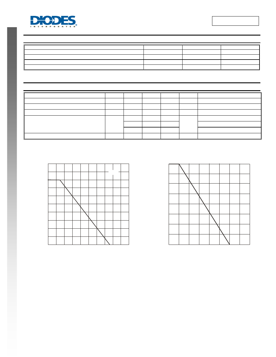
0
120
160
200
250
200
150
50
40
80
100
0
T , AMBIENT TEMPERATURE ( C)
Figure 1 Power Derating Curve
A
°
P
, P
O
WE
R
DI
SSI
P
A
T
IO
N
(mW
)
D
Note 5
0
50
25
50
75
100 125
150
P
EAK
P
U
LS
E
D
E
R
A
T
IN
G
%
O
F
PE
AK P
O
W
E
R OR
CURRENT
T , AMBIENT TEMPERATURE (°C)
Figure 2 Power Dissipation vs. Ambient Temperature
A
0
100
25
75
175 200