Maximum ratings, Thermal characteristics, Electrical characteristics – Diodes BSS127 User Manual
Page 2: Bss127
BSS127
Document number: DS35476 Rev. 6 - 2
2 of 6
January 2013
© Diodes Incorporated
BSS127
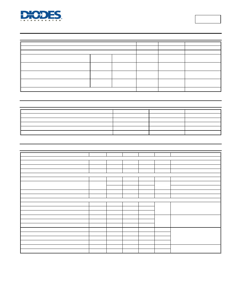
Maximum Ratings
(@T
A
= +25°C, unless otherwise specified.)
Characteristic Symbol
Value
Units
Drain-Source Voltage
V
DSS
600 V
Gate-Source Voltage
V
GSS
±20 V
Continuous Drain Current (Note 5) V
GS
= 10V
Steady
State
T
A
= +25°C
T
A
= +70°C
I
D
50
40
mA
Continuous Drain Current (Note 6) V
GS
= 10V
Steady
State
T
A
= +25°C
T
A
= +70°C
I
D
70
55
mA
Continuous Drain Current (Note 5) V
GS
= 5V
Steady
State
T
A
= +25°C
T
A
= +70°C
I
D
45
35
mA
Continuous Drain Current (Note 6) V
GS
= 5V
Steady
State
T
A
= +25°C
T
A
= +70°C
I
D
65
50
mA
Pulsed Drain Current @ T
SP
= +25°C (Notes 7)
I
DM
0.16 A
Thermal Characteristics
Characteristic Symbol
Value
Units
Power Dissipation, @T
A
= +25°C (Note 5)
P
D
0.61 W
Thermal Resistance, Junction to Ambient @ T
A
= +25°C (Note 5)
R
θJA
204 °C/W
Power Dissipation, @T
A
= +25°C (Note 6)
P
D
1.25 W
Thermal Resistance, Junction to Ambient @ T
A
= +25°C (Note 6)
R
θJA
100 °C/W
Operating and Storage Temperature Range
T
J
, T
STG
-55 to +150
°C
Electrical Characteristics
(@T
A
= +25°C, unless otherwise specified.)
Characteristic Symbol
Min
Typ
Max
Unit
Test
Condition
OFF CHARACTERISTICS (Note 8)
Drain-Source Breakdown Voltage
BV
DSS
600 — — V
V
GS
= 0V, I
D
= 250µA
Zero Gate Voltage Drain Current T
J
= +25°C
I
DSS
— — 0.1 µA
V
DS
= 600V, V
GS
= 0V
Gate-Body Leakage
I
GSS
— —
±100
nA
V
GS
= ±20V, V
DS
= 0V
ON CHARACTERISTICS (Note 8)
Gate Threshold Voltage
V
GS(th)
3 — 4.5 V
V
DS
= V
GS
, I
D
= 250µA
Static Drain-Source On-Resistance
R
DS(ON)
— 80 160
Ω
V
GS
= 10V, I
D
= 16mA
— 95 190
V
GS
= 5.0V, I
D
= 16mA
Forward Transfer Admittance
|Y
fs
|
— 76 — mS
V
DS
= 10V, I
D
= 16mA
Diode Forward Voltage
V
SD
— — 1.5 V
V
GS
= 0V, I
S
= 16mA
DYNAMIC CHARACTERISTICS (Note 9)
Input Capacitance
C
iss
— 21.8 —
pF
V
DS
= 25V, V
GS
= 0V, f = 1.0MHz
Output Capacitance
C
oss
— 2.2 —
Reverse Transfer Capacitance
C
rss
— 0.3 —
Total Gate Charge
Q
g
— 1.08 —
nC
V
GS
= 10V, V
DD
= 300V,
I
D
= 0.01A
Gate-Source Charge
Q
gs
— 0.08 —
Gate-Drain Charge
Q
gd
— 0.50 —
Turn-On Delay Time
t
D(on)
— 5.0 — ns
V
DD
= 300V, V
GS
= 10V,
R
GEN
= 6Ω,
I
D
= 10mA
Turn-On Rise Time
t
r
— 7.2 — ns
Turn-Off Delay Time
t
D(off)
— 28.7 — ns
Turn-Off Fall Time
t
f
— 168 — ns
Reverse Recovery Time
T
rr
— 131 — ns
V
R
=300 V, I
F
=0.016 A,
di/dt = 100A/µs
Reverse Recovery Charge
Q
rr
— 32 — nC
Notes:
5. Device mounted on FR-4 PCB with minimum recommended pad layout, single sided.
6. Device mounted on 1” x 1” FR-4 PCB with high coverage 2 oz. Copper, single sided.
7. Repetitive rating, pulse width limited by junction temperature, 10µs pulse, duty cycle = 1%.
8. Short duration pulse test used to minimize self-heating effect.
9. Guaranteed by design. Not subject to production testing.