Maximum ratings, Thermal characteristics, Electrical characteristics – Diodes BSS138W User Manual
Page 2: Bss138w
BSS138W
Document number: DS30206 Rev. 11 - 2
2 of 5
September 2013
© Diodes Incorporated
BSS138W
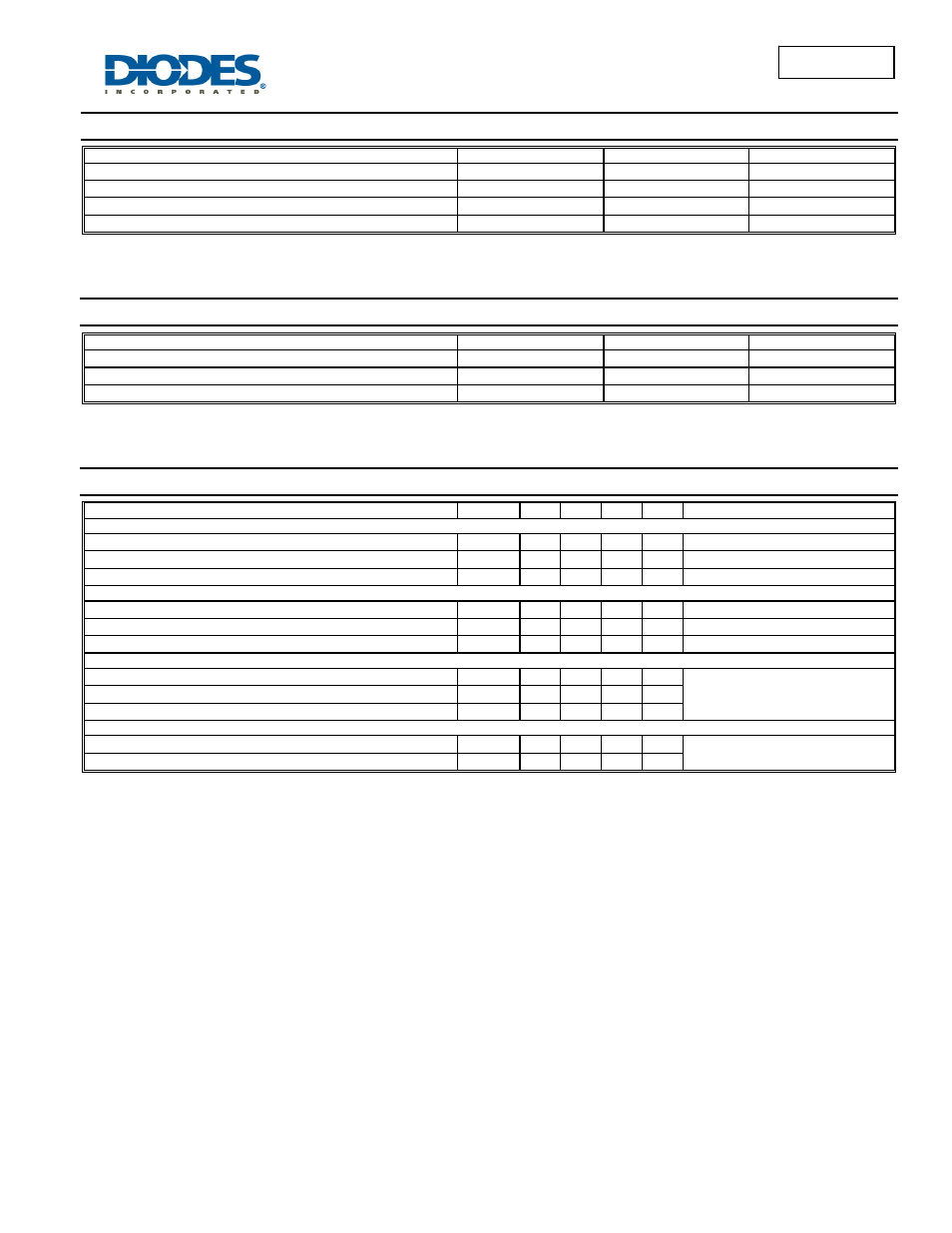
Maximum Ratings
(@T
A
= +25°C, unless otherwise specified.)
Characteristic Symbol
Value
Units
Drain-Source Voltage
V
DSS
50 V
Drain-Gate Voltage (Note 5)
V
DGR
50 V
Gate-Source Voltage
Continuous
V
GSS
20
V
Drain Current (Note 6)
Continuous
I
D
200 mA
Thermal Characteristics
(@T
A
= +25°C, unless otherwise specified.)
Characteristic Symbol
Value
Units
Total Power Dissipation (Note 6)
P
D
200 mW
Thermal Resistance, Junction to Ambient
R
JA
625
C/W
Operating and Storage Temperature Range
T
J
, T
STG
-55 to +150
C
Electrical Characteristics
(@T
A
= +25°C, unless otherwise specified.)
Characteristic Symbol
Min
Typ
Max
Unit
Test
Condition
OFF CHARACTERISTICS (Note 7)
Drain-Source Breakdown Voltage
BV
DSS
50 75
V
V
GS
= 0V, I
D
= 250
A
Zero Gate Voltage Drain Current
I
DSS
0.5 µA
V
DS
= 50V, V
GS
= 0V
Gate-Body Leakage
I
GSS
100
nA
V
GS
=
20V, V
DS
= 0V
ON CHARACTERISTICS (Note 7)
Gate Threshold Voltage
V
GS(th)
0.5 1.2 1.5 V V
DS
= V
GS
, I
D
= 250
A
Static Drain-Source On-Resistance
R
DS (ON)
1.4 3.5
V
GS
= 10V, I
D
= 0.22A
Forward Transconductance
g
FS
100
mS V
DS
= 25V, I
D
= 0.2A, f = 1.0KHz
DYNAMIC CHARACTERISTICS (Note 8)
Input Capacitance
C
iss
50 pF
V
DS
= 10V, V
GS
= 0V, f = 1.0MHz
Output Capacitance
C
oss
25 pF
Reverse Transfer Capacitance
C
rss
8.0 pF
SWITCHING CHARACTERISTICS(Note 8)
Turn-On Delay Time
t
D(ON)
20 ns
V
DD
= 30V, I
D
= 0.2A,
R
GEN
= 50
Turn-Off Delay Time
t
D(OFF)
20 ns
Notes: 5.
R
GS
20K.
6. Device mounted on FR-4 PCB, 1 inch x 0.85 inch x 0.062 inch; pad layout as shown on Diodes Inc. suggested pad layout document AP02001, which can
be found on our website at7. Short duration pulse test used to minimize self-heating effect.
8. Guaranteed by design. Not subject to production testing.