Diodes BC856AS User Manual
Bc856as, Features, Mechanical data
DS30834 Rev. 7 - 2
1 of 3
www.diodes.com
BC856AS
© Diodes Incorporated
BC856AS
DUAL PNP SURFACE MOUNT SMALL SIGNAL TRANSISTOR
Features
•
Ideally Suited for Automatic Insertion
•
For Switching and AF Amplifier Applications
•
Complementary NPN Types Available (BC846AS)
•
Lead Free/RoHS Compliant (Note 1)
•
"Green" Device (Note 4 and 5)
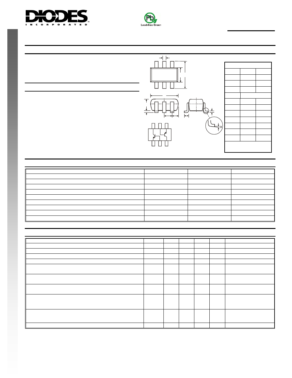
Mechanical Data
•
Case: SOT-363
•
Case Material: Molded Plastic. UL Flammability
Classification Rating 94V-0
•
Moisture Sensitivity: Level 1 per J-STD-020C
•
Terminals: Solderable per MIL-STD-202, Method 208
•
Lead Free Plating (Matte Tin Finish annealed over Alloy 42
leadframe).
•
Pin Connections: See Diagram
•
Marking Codes: See Page 3
•
Ordering & Date Code Information: See Page 3
•
Weight: 0.006 grams (approximate)
SOT-363
NEW PROD
UC
T
Dim Min Max
A
0.10 0.30
B
1.15 1.35
C
2.00 2.20
D
0.65 Nominal
F
0.30 0.40
H
1.80 2.20
J
⎯
0.10
K
0.90 1.00
L
0.25 0.40
M
0.10 0.25
α
0
°
8°
All Dimensions in mm
Maximum Ratings
@T
A
= 25°C unless otherwise specified
Characteristic Symbol
Value
Unit
Collector-Base Voltage
V
CBO
-80 V
Collector-Emitter Voltage
V
CEO
-65 V
Emitter-Base Voltage
V
EBO
-5.0 V
Collector Current
I
C
-100 mA
Peak Collector Current
I
CM
-200 mA
Peak Emitter Current
I
EM
-200 mA
Power Dissipation (Note 2)
P
d
200 mW
Thermal Resistance, Junction to Ambient (Note 2)
R
θJA
625 °C/W
Operating and Storage Temperature Range
T
j
, T
stg
-65 to +150
°C
Electrical Characteristics
@T
A
= 25°C unless otherwise specified
Characteristic Symbol
Min
Typ
Max
Unit
Test
Condition
Collector-Base Breakdown Voltage (Note 3)
V
(BR)CBO
-80 — — V
I
C
= 10
μA, I
B
= 0
Collector-Emitter Breakdown Voltage (Note 3)
V
(BR)CEO
-65 — — V
I
C
= 10mA, I
B
= 0
Emitter-Base Breakdown Voltage (Note 3)
V
(BR)EBO
-5 — — V
I
E
= 1
μA, I
C
= 0
DC Current Gain (Note 3)
h
FE
125 180 250 —
V
CE
= -5.0V, I
C
= -2.0mA
Collector-Emitter Saturation Voltage (Note 3)
V
CE(SAT)
—
-75
-250
-300
-650
mV
I
C
= -10mA, I
B
= -0.5mA
I
C
= -100mA, I
B
= -5.0mA
Base-Emitter Saturation Voltage (Note 3)
V
BE(SAT)
—
—
-700
-850
— mV
I
C
= -10mA, I
B
= -0.5mA
I
C
= -100mA, I
B
= -5.0mA
Base-Emitter Voltage (Note 3)
V
BE(ON)
-600
—
-650
—
-750
-820
mV
V
CE
= -5.0V, I
C
= -2.0mA
V
CE
= -5.0V, I
C
= -10mA
Collector-Cutoff Current (Note 3)
I
CES
I
CBO
I
CBO
—
—
—
—
—
—
-15
-15
-4.0
nA
nA
µA
V
CE
= -80V
V
CB
= -30V
V
CB
= -30V, T
A
= 150°C
Gain Bandwidth Product
f
T
100 — — MHz
V
CE
= -5.0V, I
C
= -10mA,
f = 100MHz
Collector-Base Capacitance
C
CB
— 3 — pF
V
CB
= -10V, f = 1.0MHz
Notes:
1. No purposefully added lead.
2. Device mounted on FR-4 PCB; pad layout as shown on page 3 or on Diodes Inc. suggested pad layout document AP02001, which can be found on our
website at .
3. Short duration pulse test used to minimize self-heating effect.
4. Diodes Inc.'s "Green" policy can be found on our website at http://www.diodes.com/products/lead_free/index.php.
5. Product manufactured with Date Code UO (week 40, 2007) and newer are built with Green Molding Compound. Product manufactured prior to Date
Code UO are built with Non-Green Molding Compound and may contain Halogens or Sb2O3 Fire Retardants.
C
1
6
5
4
3
2
1
B
2
E
2
E
1
B
1
C
2
A
M
J
L
D
C
B
H
K
F
Top View