Diodes BC847BVC User Manual
Features, Mechanical data, Maximum ratings
BC847BVC
Document number: DS30638 Rev. 5 - 2
1 of 4
April 2009
© Diodes Incorporated
BC847BVC
NPN DUAL SMALL SIGNAL SURFACE MOUNT TRANSISTOR
Features
•
Epitaxial Die Construction
•
Ultra-Small Surface Mount Package
•
Lead Free By Design/RoHS Compliant (Note 3)
•
"Green" Device (Note 4)
•
Qualified to AEC-Q101 Standards for High Reliability
Mechanical Data
• Case:
SOT-563
•
Case Material: Molded Plastic, "Green" Molding Compound. UL
Flammability Classification Rating 94V-0
•
Moisture Sensitivity: Level 1 per J-STD-020D
•
Terminal Connections: See Diagram
•
Terminals: Finish - Matte Tin annealed over Copper leadframe.
Solderable per MIL-STD-202, Method 208
•
Marking Information: See Page 2
•
Ordering Information: See Page 2
•
Weight: 0.002 grams (approximate)
Maximum Ratings
@T
A
= 25°C unless otherwise specified
Characteristic
Symbol
Value
Unit
Collector-Base Voltage
V
CBO
50
V
Collector-Emitter Voltage
V
CEO
45
V
Emitter-Base Voltage
V
EBO
6.0
V
Collector Current
I
C
100
mA
Thermal Characteristics
Characteristic
Symbol
Value
Unit
Power Dissipation (Note 2)
P
D
150
mW
Thermal Resistance, Junction to Ambient (Note 2)
R
θJA
833
°C/W
Operating and Storage Temperature Range
T
J
, T
STG
-55 to +150
°C
Electrical Characteristics
@T
A
= 25°C unless otherwise specified
Characteristic
Symbol
Min
Typ
Max
Unit
Test Condition
Collector-Base Breakdown Voltage (Note 5)
V
(BR)CBO
50
—
—
V
I
C
= 10
μA, I
B
= 0
Collector-Emitter Breakdown Voltage (Note 5)
V
(BR)CEO
45
—
—
V
I
C
= 10mA, I
B
= 0
Emitter-Base Breakdown Voltage (Note 5)
V
(BR)EBO
6
—
—
V
I
E
= 1
μA, I
C
= 0
DC Current Gain (Note 5)
h
FE
200
290
450
—
V
CE
= 5.0V, I
C
= 2.0mA
Collector-Emitter Saturation Voltage (Note 5)
V
CE(SAT)
—
—
100
300
mV
I
C
= 10mA, I
B
= 0.5mA
I
C
= 100mA, I
B
= 5.0mA
Base-Emitter Saturation Voltage (Note 5)
V
BE(SAT)
—
700
900
—
mV
I
C
= 10mA, I
B
= 0.5mA
I
C
= 100mA, I
B
= 5.0mA
Base-Emitter Voltage (Note 5)
V
BE
580
—
660
—
700
770
mV
V
CE
= 5.0V, I
C
= 2.0mA
V
CE
= 5.0V, I
C
= 10mA
Collector-Emitter Cutoff Current (Note 5)
I
CBO
I
CBO
—
—
15
5.0
nA
µA
V
CB
= 30V
V
CB
= 30V, T
A
= 150°C
Gain Bandwidth Product
f
T
100
—
—
MHz
V
CE
= 5.0V, I
C
= 10mA,
f = 100MHz
Output Capacitance
C
OBO
—
—
4.5
pF
V
CB
= 10V, f = 1.0MHz
Noise Figure
NF
—
—
10
dB
V
CE
= 5V, R
S
= 2.0k
Ω,
f = 1.0kHz, BW
= 200Hz
Notes:
1. Package is non-polarized. Parts may be on reel in orientation illustrated, 180° rotated, or mixed (both ways).
2. Device mounted on FR-4 PCB, 1 inch x 0.85 inch x 0.062 inch; pad layout as shown on Diodes Inc. suggested pad layout document AP02001, which
can be found on our website3. No purposefully added lead.
4. Diodes Inc's "Green" policy can be found on our webs5. Short duration pulse test used to minimize self-heating effect.
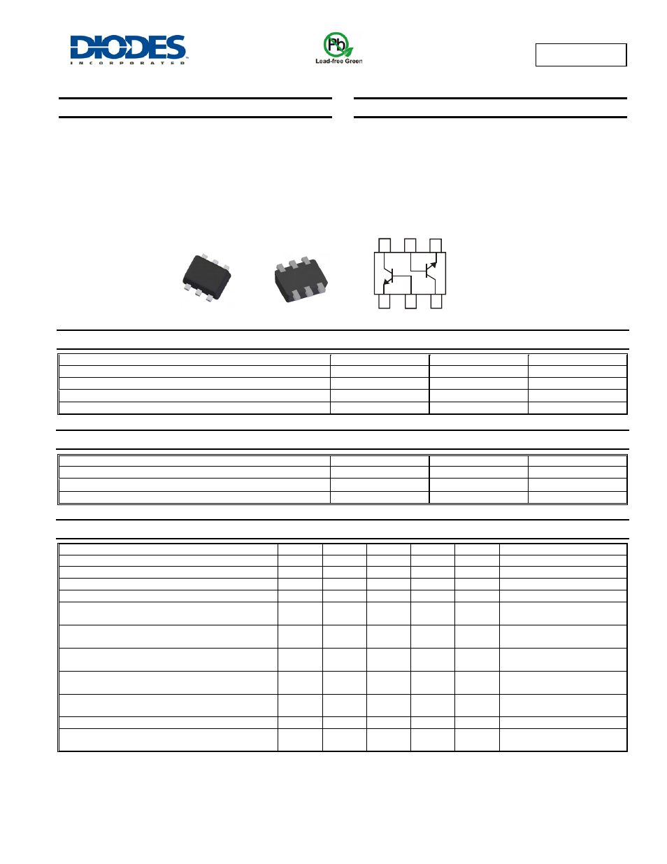
Top View
Bottom View
Device Schematic
C
1
B
2
E
2
C
2
E
1
B
1