Absolute maximum ratings, Thermal characteristics, Esd ratings – Diodes BC807-16W/ -25W/ -40W User Manual
Page 2: Electrical characteristics
BC807-16W/-25W/-40W
Document Number: DS30577 Rev. 7 - 2
2 of 5
November 2013
© Diodes Incorporated
BC807-16W/ -25W/ -40W
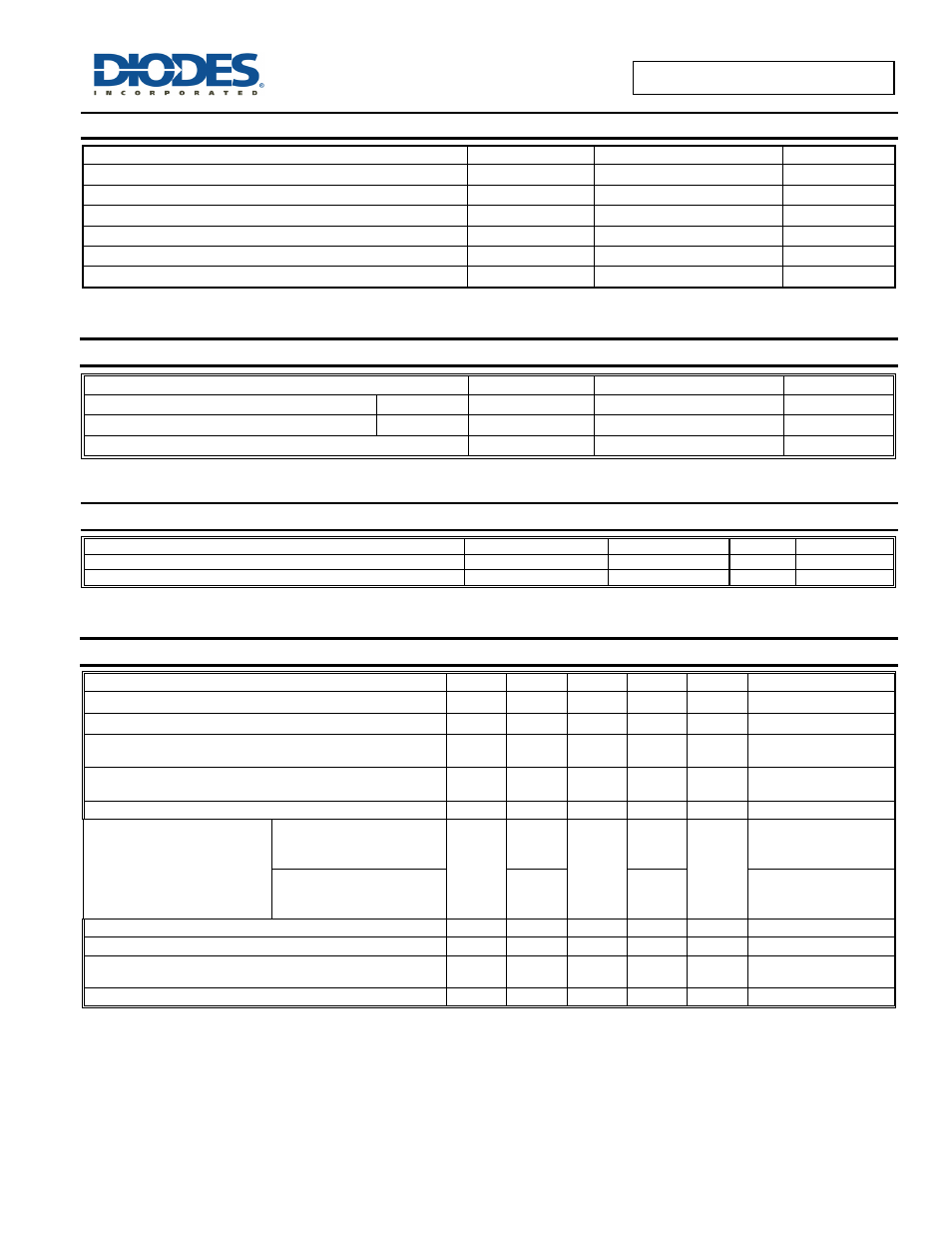
Absolute Maximum Ratings
(@T
A
= +25°C, unless otherwise specified.)
Characteristic Symbol
Value
Unit
Collector-Base Voltage
V
CBO
-50 V
Collector-Emitter Voltage
V
CEO
-45 V
Emitter-Base Voltage
V
EBO
-6 V
Continuous Collector Current
I
C
-500 mA
Peak Collector Current
I
CM
-1.0 A
Peak Base Current
I
BM
-200 mA
Thermal Characteristics
(@T
A
= +25°C, unless otherwise specified.)
Characteristic Symbol
Value
Unit
Power Dissipation
(Note 5)
P
D
200 mW
Thermal Resistance, Junction to Ambient
(Note 5)
R
θJA
625
C/W
Operating and Storage Temperature Range
T
J,
T
STG
-65 to +150
C
ESD Ratings
(Note 6)
Characteristic Symbol
Value
Unit
JEDEC
Class
Electrostatic Discharge - Human Body Model
ESD HBM
4,000
V
3A
Electrostatic Discharge - Machine Model
ESD MM
400
V
C
Electrical Characteristics
(@T
A
= +25°C, unless otherwise specified.)
Characteristic
Symbol
Min
Typ
Max
Unit
Test Condition
Collector-Emitter Breakdown Voltage (Note 7)
BV
CEO
-45
—
—
V
I
C
= -10mA
Emitter-Base Breakdown Voltage
BV
EBO
-6
—
—
V
I
C
= -100µA
Collector-Emitter Cutoff Current
I
CES
—
—
-100
-5.0
nA
µA
V
CE
= -45V
V
CE
= -25V, T
J
= +150°C
Collector
I
CBO
—
—
-100
-5.0
nA
µA
V
CB
= -20V
V
CB
= -20V, T
J
= +150°C
Emitter-Base Cutoff Current
I
EBO
—
—
-100
nA
V
EB
= -5V
DC Current Gain (Note 7)
BC807-16W-7
BC807-25W-7
BC807-40W-7
h
FE
100
160
250
—
250
400
600
—
I
C
= -100mA, V
CE
= -1.0V
BC807-16W-7
BC807-25W-7
BC807-40W-7
60
100
170
—
I
C
= -300mA, V
CE
= -1.0V
Collector-Emitter Saturation Voltage (Note 7)
V
CE(sat)
—
—
-700
mV
I
C
= -500mA, I
B
= -50mA
Base-Emitter Voltage (Note 7)
V
BE
—
—
-1200
mV
I
C
= -300mA, V
CE
= -1.0V
Gain Bandwidth Product
f
T
100
—
—
MHz
V
CE
= -5.0V, I
C
= -10mA,
f = 50MHz
Collector-Base Capacitance
C
CBO
—
—
12
pF
V
CB
= -10V, f = 1.0MHz
Notes:
5. For a device mounted on minimum recommended pad layout 1oz copper that is on a single-sided FR4 PCB; device is measured under still air
conditions whilst operating in a steady-state.
6. Refer to JEDEC specification JESD22-A114 and JESD22-A115.
7. Measured under pulsed conditions. Pulse width ≤ 300µs. Duty cycle ≤ 2%.