Maximum ratings, Thermal characteristics – Diodes 2DD1664P/Q/R User Manual
Page 2
2DD1664P/Q/R
Document number: DS31143 Rev. 5 - 2
2 of 6
July 2012
© Diodes Incorporated
2DD1664P/Q/R
Maximum Ratings
(@T
A
= +25°C, unless otherwise specified.)
Characteristic Symbol
Value
Unit
Collector-Base Voltage
V
CBO
40 V
Collector-Emitter Voltage
V
CEO
32 V
Emitter-Base Voltage
V
EBO
6 V
Continuous Collector Current
I
C
1 A
Peak Pulse Current (Note 6)
I
CM
2 A
Thermal Characteristics
Characteristic Symbol
Value
Unit
Power Dissipation (Note 5)
P
D
1 W
Thermal Resistance, Junction to Ambient (Note 5)
R
θJA
125
°C/W
Thermal Resistance, Junction to Leads (Note 7)
R
θJL
22
°C/W
Operating and Storage Temperature Range
T
J,
T
STG
-55 to +150
°C
Notes:
5. For a device surface mounted on FR-4 PCB with minimum suggested pad layout; high coverage of single sided 1 oz copper, in still air conditions
6. Measured under pulsed conditions. Pulse width = 300µs. Duty cycle
≤ 2%.
7. Thermal resistance from junction to solder-point (at the end of the collector lead).
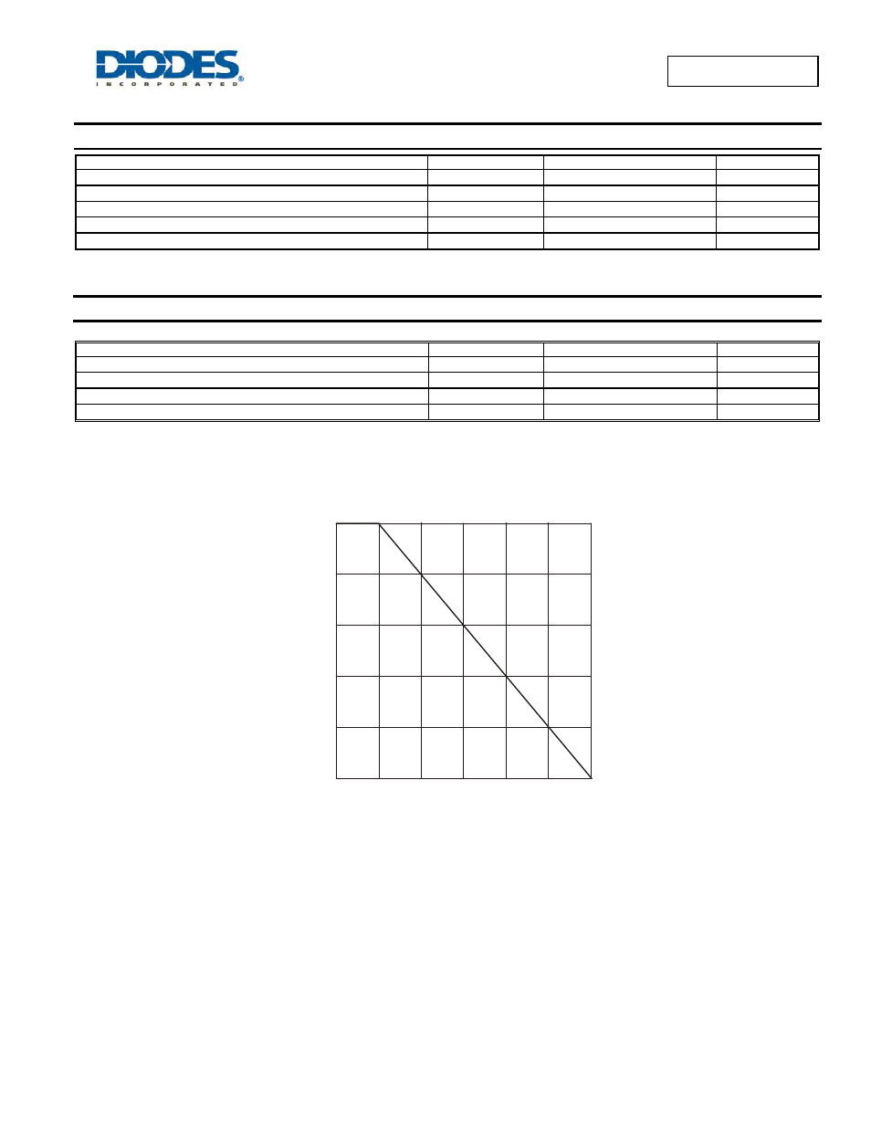
0
0.2
0.4
25
50
75
100
125
150
P
,
P
O
WE
R
DIS
S
IP
A
T
IO
N
(W
)
D
T , AMBIENT TEMPERATURE (°C)
A
Figure 1. Power Dissipation vs. Ambient Temperature
0.6
0.8
1.0
0