Maximum ratings, Thermal characteristics, Electrical characteristics – Diodes 2DC4617QLP User Manual
Page 2
2DC4617QLP
Document number: DS31439 Rev. 4 - 2
2 of 5
February 2011
© Diodes Incorporated
2DC4617QLP
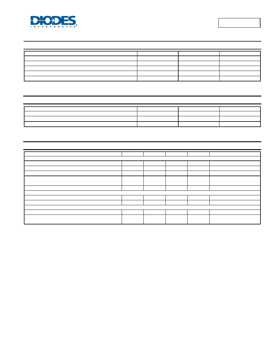
Maximum Ratings
@T
A
= 25°C unless otherwise specified
Characteristic Symbol
Value
Unit
Collector-Base Voltage
V
CBO
50 V
Collector-Emitter Voltage
V
CEO
50 V
Emitter-Base Voltage
V
EBO
5.0 V
Collector Current - Continuous
I
C
100 mA
Peak Collector Current
I
CM
200 mA
Thermal Characteristics
@T
A
= 25°C unless otherwise specified
Characteristic Symbol
Value
Unit
Power Dissipation (Note 4)
P
D
250 mW
Thermal Resistance, Junction to Ambient (Note 4)
R
θJA
500
°C/W
Operating and Storage Temperature Range
T
J
, T
STG
-55 to +150
°C
Electrical Characteristics
@T
A
= 25°C unless otherwise specified
Characteristic Symbol
Min
Max
Unit
Test
Condition
OFF CHARACTERISTICS (Note 5)
Collector-Base Breakdown Voltage
V
(BR)CBO
50
⎯
V
I
C
= 50
μA, I
E
= 0
Collector-Emitter Breakdown Voltage
V
(BR)CEO
50
⎯
V
I
C
= 1.0mA, I
B
= 0
Emitter-Base Breakdown Voltage
V
(BR)EBO
5.0
⎯
V
I
E
= 50
μA, I
C
= 0
Collector Cutoff Current
I
CBO
⎯
100
5
nA
μA
V
CB
= 30V
V
CB
= 30V, T
A
= 150°C
Emitter Cutoff Current
I
EBO
⎯
100 nA
V
EB
= 4.0V
ON CHARACTERISTICS (Note 5)
DC Current Gain
h
FE
120 270
⎯
V
CE
= 6.0V, I
C
= 1.0mA
Collector-Emitter Saturation Voltage
V
CE(SAT)
⎯
0.2 V
I
C
= 50mA, I
B
= 5.0mA
SMALL SIGNAL CHARACTERISTICS
Output Capacitance
C
obo
⎯
3.5 pF
V
CB
= 12V, f = 1.0MHz, I
E
= 0
Current Gain-Bandwidth Product
f
T
100
⎯
MHz
V
CE
= 12V, I
C
= 2.0mA,
f = 100MHz
Notes:
4. Part mounted on FR-4 PCB with recommended pad layout.
5. Short duration pulse test used to minimize self-heating effect.