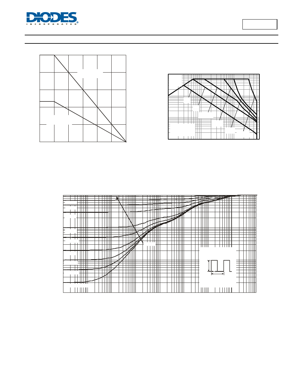
Safe operating area, Thermal characteristics and derating information, Co lle ct o r cu rre n t (a ) -v – Diodes 2DA1797 User Manual
Page 3: Collector-emitter voltage (v)
2DA1797
Document number: DS31619 Rev. 4 - 2
3 of 7
November 2013
© Diodes Incorporated
2DA1797
NEW PROD
UC
T
Thermal Characteristics and Derating Information
(@T
A
= +25°C, unless otherwise specified.)
100m
1
10
10m
100m
1
10
100µs
Single Pulse
T
amb
=25°C
V
CE(sat)
Limited
1ms
10ms
100ms
1s
DC
Safe Operating Area
-I
C
Co
lle
ct
o
r
Cu
rre
n
t (A
)
-V
CE
Collector-Emitter Voltage (V)
0
0.4
0.8
25
50
75
100
125
150
P
,
P
O
WE
R
DISS
IP
A
T
IO
N (
W
)
D
T , AMBIENT TEMPERATURE (°C)
Fig. 1 Power Dissipation vs.
Ambient Temperature
A
1.2
1.6
2.0
0
FR-4 PCB
1 inch copper pad
2
FR-4 PCB
Minimum
recommended pad
0.00001
0.0001
0.001
0.01
0.1
1
10
100
1,000
Fig. 10 Transient Thermal Response
t , PULSE DURATION TIME (s)
1
0.001
0.01
0.1
1
r(
t), T
R
A
N
S
IE
NT
T
H
E
R
M
A
L R
E
S
IS
TA
N
C
E
T - T = P * R
(t)
Duty Cycle, D = t /t
J
A
JA
1 2
R
(t) = r(t) *
JA
R
R
= 126°C/W
JA
JA
P(pk)
t
1
t
2
D = 0.7
D = 0.3
D = 0.1
D = 0.05
D = 0.02
D = 0.01
D = 0.005
D = Single Pulse
D = 0.9
D = 0.5