Maximum ratings, Thermal characteristics, Electrical characteristics – Diodes DCX69/-16/-25 User Manual
Page 2
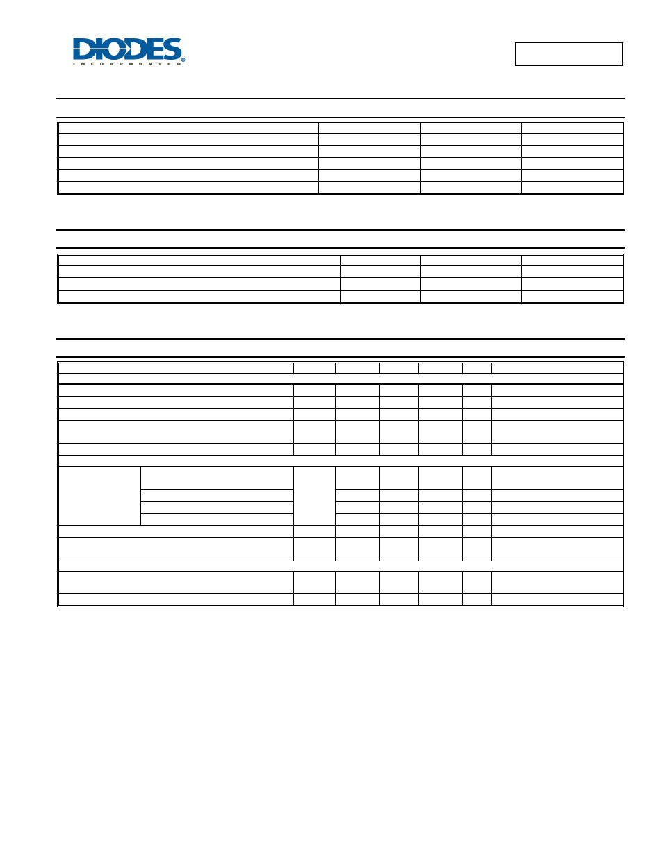
DCX69/-16/-25
Document number: DS31264 Rev. 6 - 2
2 of 5
April 2012
© Diodes Incorporated
DCX69/-16/-25
Maximum Ratings
@T
A
= 25°C unless otherwise specified
Characteristic Symbol
Value
Unit
Collector-Base Voltage
V
CBO
-25 V
Collector-Emitter Voltage
V
CEO
-20 V
Emitter-Base Voltage
V
EBO
-5.0 V
Collector Current
I
C
-1.0 A
Peak Pulse Power
I
CM
-2.0 A
Thermal Characteristics
Characteristic Symbol
Value
Unit
Power Dissipation (Note 4) @ T
A
= 25°C
P
D
1 W
Thermal Resistance, Junction to Ambient Air @ T
A
= 25°C (Note 4)
R
θJA
125 °C/W
Operating and Storage Temperature Range
T
J
, T
STG
-55 to +150
°C
Electrical Characteristics
@T
A
= 25°C unless otherwise specified
Characteristic Symbol
Min
Typ
Max
Unit
Test
Conditions
OFF CHARACTERISTICS (Note 5)
Collector-Base Breakdown Voltage
V
(BR)CBO
-25
⎯
⎯
V
I
C
= -100
μA, I
E
= 0
Collector-Emitter Breakdown Voltage
V
(BR)CEO
-20
⎯
⎯
V
I
C
= -10mA, I
B
= 0
Emitter-Base Breakdown Voltage
V
(BR)EBO
-5.0
⎯
⎯
V
I
E
= -100
μA, I
C
= 0
Collector-Base Cutoff Current
I
CBO
⎯
⎯
-100
-10
nA
μA
V
CB
= -25V, I
E
= 0
V
CB
= -25V, I
E
= 0, T
A
= 150°C
Emitter-Base Cutoff Current
I
EBO
⎯
⎯
-100 nA
V
EB
= -5.0V, I
C
= 0
ON CHARACTERISTICS (Note 5)
DC Current Gain
DCX69, DCX69-16, DCX69-25
h
FE
50
60
⎯
⎯
⎯
⎯
⎯
⎯
V
CE
= -10V, I
C
= -5.0mA
V
CE
= -1.0V, I
C
= -1.0A
DCX69
85
⎯
375
⎯ V
CE
= -1.0V, I
C
= -500mA
DCX69-16
100
⎯
250
⎯ V
CE
= -1.0V, I
C
= -500mA
DCX69-25
160
⎯
375
⎯ V
CE
= -1.0V, I
C
= -500mA
Collector-Emitter Saturation Voltage
V
CE(SAT)
⎯
⎯
-0.5 V
I
C
= -1.0A, I
B
= -100mA
Base-Emitter Turn-On Voltage
V
BE(ON)
⎯
⎯
⎯
-0.7
-1.0
V
V
CE
= -10V, I
C
= -5mA
V
CE
= -1.0V, I
C
= -500mA
SMALL SIGNAL CHARACTERISTICS
Current Gain-Bandwidth Product
f
T
40 200
⎯
MHz
V
CE
= -5.0V, I
C
= -50mA,
f = 100MHz
Output Capacitance
C
obo
⎯
17
⎯
pF
V
CB
= -10V, f = 1MHz
Notes:
4. Device mounted on FR-4 PCB; pad layout as shown on Diodes Inc. suggested pad layout document AP02001, which can be found on our website at
5. Measured under pulsed conditions. Pulse width = 300
μs. Duty cycle ≤2%.