Maximum ratings, Thermal characteristics – Diodes 2DA2018 User Manual
Page 2
2DA2018
Document number: DS31823 Rev. 3 - 2
2 of 5
October 2010
© Diodes Incorporated
2DA2018
ADVAN
CE I
N
F
O
RM
ATI
O
N
Maximum Ratings
@T
A
= 25°C unless otherwise specified
Characteristic Symbol
Value
Unit
Collector-Base Voltage
V
CBO
-15 V
Collector-Emitter Voltage
V
CEO
-12 V
Emitter-Base Voltage
V
EBO
-6 V
Collector Current - Continuous
I
C
-500 mA
Peak Pulse Collector Current
I
CM
-1 A
Thermal Characteristics
Characteristic Symbol
Value
Unit
Power Dissipation (Note 4) @ T
A
= 25
°C P
D
150 mW
Thermal Resistance, Junction to Ambient (Note 4) @ T
A
= 25
°C
R
θJA
833
°C/W
Operating and Storage Temperature Range
T
J
, T
STG
-55 to +150
°C
Notes:
4. Device mounted on FR-4 PCB with minimum recommended pad layout.
0
20
40
60
80
100
120
140
160
P
, P
OW
E
R
DI
S
S
IP
A
T
ION
(mW
)
D
0
20
40
60
80
100
120
140
160
T , AMBIENT TEMPERATURE ( C)
A
°
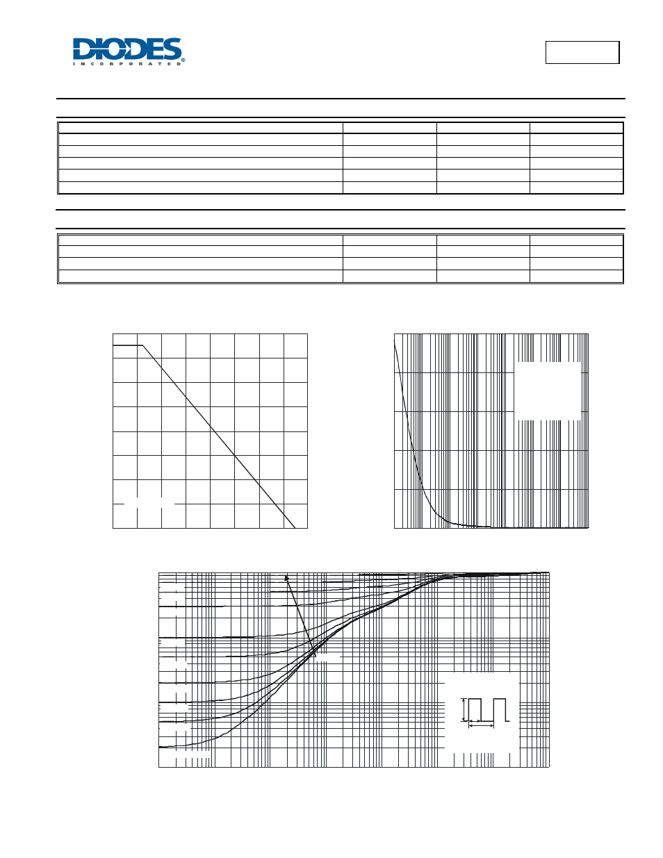
Fig. 1 Power Dissipation vs. Ambient Temperature
R
= 833°C/W
θJA
0
20
40
60
80
100
0.0001 0.001
0.1
10
1,000
Fig. 2 Single Pulse Maximum Power Dissipation
t , PULSE DURATION TIME (s)
1
0.01
1
100
Single Pulse
T - T = P * R
(t)
Duty Cycle, D = t /t
J
A
JA
1 2
θ
R
(t) = r(t) *
θJA
R
R
= 470°C/W
θ
θ
JA
JA
P
(p
k
),
P
EA
K
T
R
A
N
SI
E
N
T
P
O
WE
R
(W
)
0.0001
0.001
0.01
0.1
1
10
100
1,000
Fig. 3 Transient Thermal Response
t , PULSE DURATION TIME (s)
1
0.001
0.01
0.1
1
r(t),
T
R
ANSI
E
N
T
T
H
E
R
MA
L
R
ES
IS
T
AN
C
E
T - T = P * R
(t)
Duty Cycle, D = t /t
J
A
JA
1 2
θ
R
(t) = r(t) *
θJA
R
R
= 470°C/W
θ
θ
JA
JA
P(pk)
t
1
t
2
D = 0.7
D = 0.5
D = 0.3
D = 0.05
D = 0.02
D = 0.01
D = 0.005
D = Single Pulse
D = 0.9
D = 0.1