Maximum ratings, Thermal characteristics, Electrical characteristics – Diodes D3Z2V4BF – D3Z36BF User Manual
Page 2
D3Z2V4BF – D3Z36BF
Document number: DS35437 Rev. 7 - 2
2 of 5
October 2012
© Diodes Incorporated
D3Z2V4BF – D3Z36BF
NEW PROD
UC
T
NEW PROD
UC
T
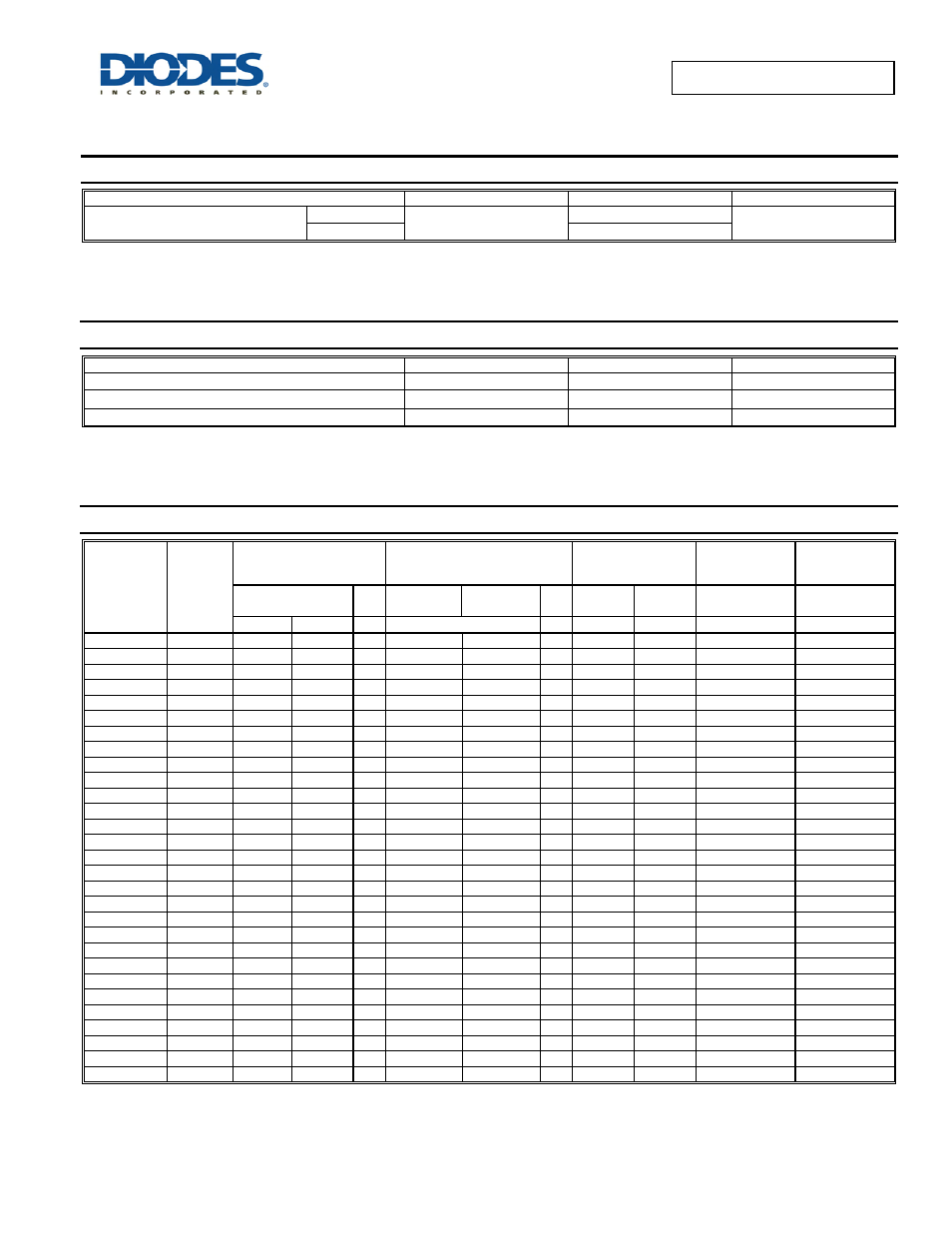
Maximum Ratings
(@T
A
= +25°C, unless otherwise specified.)
Characteristic Symbol
Value
Unit
Forward Voltage
@ I
F
= 10mA
V
F
0.9
V
@ I
F
= 100mA
1.1
Thermal Characteristics
Characteristic Symbol
Value
Unit
Power Dissipation (Note 5)
P
D
400 mW
Thermal Resistance, Junction to Ambient Air (Note 5)
R
θJA
312.5
°C/W
Operating and Storage Temperature Range
T
J,
T
STG
-65 to +150
°C
Electrical Characteristics
(@T
A
= +25°C, unless otherwise specified.)
Type
Number
Marking
Code
Zener Voltage Range
(Note 6)
Maximum Zener Impedance
f = 1kHz
Maximum Reverse
Current (Note 7)
Typical
Temperature
Coefficient
Typical Total
Capacitance
V
Z
@
I
ZT
I
ZT
Z
ZT
@
I
ZT
Z
ZK
@
I
ZK
I
ZK
I
R
@
V
R
@
I
ZT
= 5mA
@ V
R
= 0V,
f=1MHz
Min (V)
Max (V) mA
Ω
mA
μA
V mV/°C
pF
D3Z2V4BF L0 2.43 2.63
5 100
1000 0.5
50
1
-1.6
215
D3Z2V7BF L1 2.69 2.91
5 100
1000 0.5
20
1
-1.7
205
D3Z3V0BF L2 2.85 3.07
5 95
1000 0.5
10
1
-1.7
195
D3Z3V3BF L3 3.32 3.53
5 95
1000 0.5 5
1
-1.9
145
D3Z3V6BF L4 3.60 3.85 5 90
500 1.0 5
1
-2.4
185
D3Z3V9BF L5 3.89 4.16 5 90
500 1.0 3
1
-2.5
175
D3Z4V3BF L6 4.17 4.48 5 90
600 1.0 3
1
-2.5
165
D3Z4V7BF L7 4.55 4.75 5 90
600 1.0 2
1
-1.1
150
D3Z5V1BF
GM,
L8
4.96 5.20 5 60
250 0.5 2
1.5
0.3
145
D3Z5V6BF L9 5.48 5.73 5 50
100 0.5 1
2.5
1.7
20
D3Z6V2BF LA 6.06 6.33 5 50
80 0.5
0.5
3
2.5
95
D3Z6V8BF LB 6.65 6.93 5 40
60 0.5
0.5 3.5
3.4
82
D3Z7V5BF LC 7.28 7.60 5 10
60 0.5
0.5
4
4.0
70
D3Z8V2BF LD 8.02 8.36 5 10
60 0.5
0.5
5
4.6
57
D3Z9V1BF LE 8.85 9.23 5 10
60 0.5
0.5
6
5.0
50
D3Z10BF LF 9.77
10.21
5 10
60 0.5
0.1 7
6.1
45
D3Z11BF LG 10.78
11.22
5 10
60 0.5
0.1 8
7.4
41
D3Z12BF LH 11.74
12.24
5 10
80 0.5
0.1 9
8.2
36
D3Z13BF LJ 12.91
13.49
5 10
80 0.5
0.1 10
9.4
33
D3Z15BF LK 14.34
14.98
5 15
80 0.5
0.05 11
12.1
28
D3Z16BF LL 15.85
16.51
5 20
80 0.5
0.05 12
13.7
25
D3Z18BF LM 17.56
18.35
5 20
80 0.5
0.05 13
15.8
24
D3Z20BF LN 19.52
20.39
5 20
100 0.5
0.05 15
16.4
22
D3Z22BF LP 21.54
22.47
5 25
100 0.5
0.05 17
18.4
20
D3Z24BF LQ 23.72
24.78
5 30
120 0.5
0.05 19
20.4
18
D3Z27BF LR 26.19
27.53
5 40
150 0.5
0.05 21
18.0
17
D3Z30BF LS 29.19
30.69
5 40
200 0.5
0.05 23
28.6
17
D3Z33BF LT 32.15
33.79
5 40
250 0.5
0.05 25
32.2
15
D3Z36BF LU 35.07
36.87
5 60
300 0.5
0.05 27
34.9
14
Notes:
5. Device mounted on FR-4 PCB with suggested pad layout, board size 35mm * 25mm.
6. The Zener voltage is measured 40ms after power is supplied.
7. Short duration pulse test used to minimize self-heating effect.