Marking information, Package outline dimensions, Ordering information – Diodes BZX84C2V4S - BZX84C39S User Manual
Page 3: Kxx ym kxx y m
BZX84C2V4S - BZX84C39S
BZX84C2V4S - BZX84C39S
Document number: DS30108 Rev. 17 - 2
3 of 4
www.diodes.com
May 2008
© Diodes Incorporated
0
10
20
30
0
I,
Z
E
N
E
R
C
U
R
R
EN
T
(mA
)
Z
V , ZENER VOLTAGE (V)
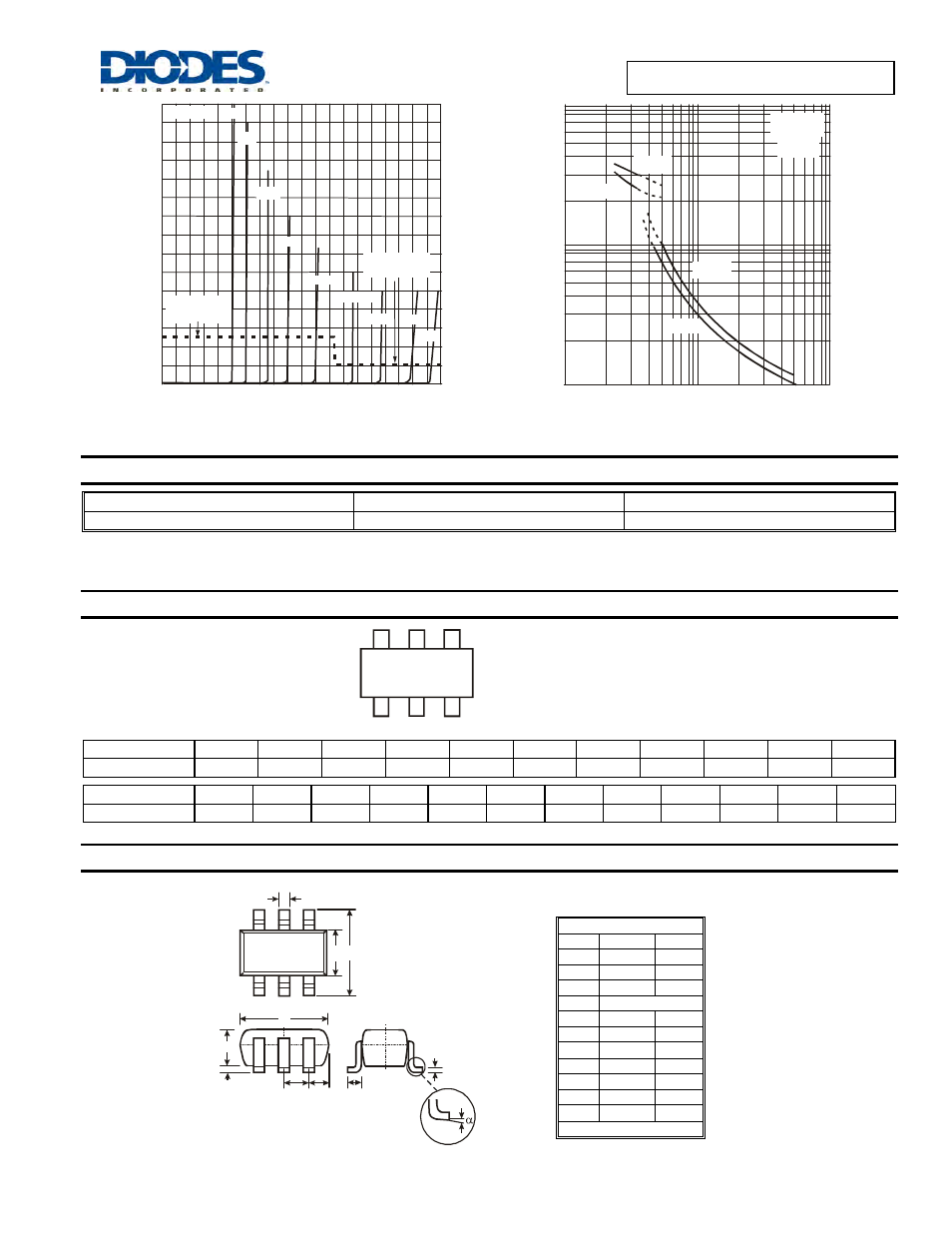
Fig. 3 Typical Zener Breakdown Characteristics
Z
10
20
30
40
T = 25°C
J
Test current I
5mA
Z
Test current I
2mA
Z
C10
C12
C18
C22
C27
C33
C36
C15
C39
C
, T
O
T
A
L
C
A
P
A
CIT
A
NCE
(p
F
)
T
10
100
1,000
10
100
1
V , NOMINAL ZENER VOLTAGE (V)
Fig. 4 Typical Total Capacitance vs. Nominal Zener Voltage
Z
T = 25 °C
J
f = 1MHz
V = 1V
R
V = 2V
R
V = 1V
R
V = 2V
R
Ordering Information
(Note 7)
Part Number
Case
Packaging
(Type Number)-7-F*
SOT-363
3000/Tape & Reel
*Add “-7-F” to the appropriate type number in Electrical Characteristics Table from Page 2 example: 6.2V Zener = BZX84C6V2S-7-F.
Notes:
7. For packaging details, go to our website at.
Marking Information
Kxx YM
Kxx Y
M
Kxx = Product Type Marking Code
(See Electrical Characteristics Table)
YM = Date Code Marking
Y = Year (ex: N = 2002)
M = Month (ex: 9 = September)
Date Code Key
Year
2002
2003
2004
2005
2006
2007
2008
2009
2010
2111
2012
Code
N
P
R
S
T
U
V
W
X
Y
Z
Month
Jan
Feb
Mar
Apr
May
Jun
Jul
Aug
Sep
Oct
Nov
Dec
Code
1 2 3 4 5 6 7 8 9 O N D
Package Outline Dimensions
A
M
J
L
D
B C
H
K
F
SOT-363
Dim
Min
Max
A
0.10
0.30
B
1.15
1.35
C
2.00
2.20
D
0.65 Nominal
F
0.30
0.40
H
1.80
2.20
J
⎯
0.10
K
0.90
1.00
L
0.25
0.40
M
0.10
0.25
α
0° 8°
All Dimensions in mm