Maximum ratings, Thermal characteristics, Electrical characteristics – Diodes BZT52C2V0 - BZT52C51 User Manual
Page 2
BZT52C2V0 - BZT52C51
Document number: DS18004 Rev. 37 - 2
2 of 5
September 2012
© Diodes Incorporated
BZT52C2V0 - BZT52C51
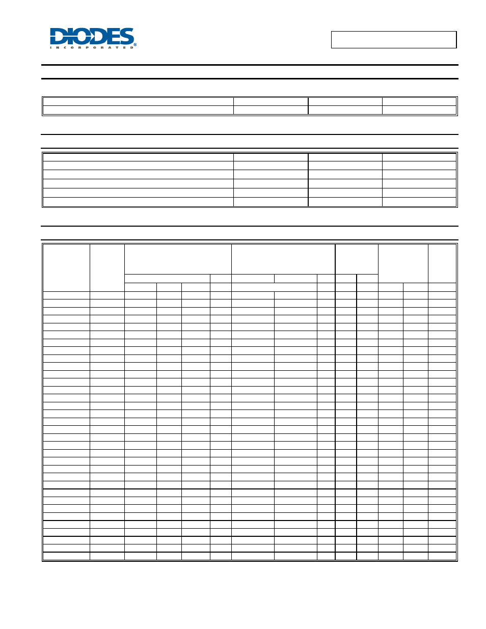
Maximum Ratings
(@T
A
= +25°C, unless otherwise specified.)
Single phase, half wave, 60Hz, resistive or inductive load.
For capacitance load, derate current by 20%.
Characteristic Symbol
Value
Unit
Forward Voltage
@ I
F
= 10mA
V
F
0.9 V
Thermal Characteristics
Characteristic Symbol
Value
Unit
Power Dissipation (Note 7) @T
L
= +75°C
P
D
500 mW
Power Dissipation (Note 8) @T
A
= +25°C
P
D
370 mW
Thermal Resistance, Junction to Ambient Air (Note 8)
R
θJA
338
°C/W
Thermal Resistance, Junction to Lead (Note 9)
R
θJL
150
°C/W
Operating and Storage Temperature Range
T
J,
T
STG
-65 to +150
°C
Electrical Characteristics
(@T
A
= +25°C, unless otherwise specified.)
Type
Number
Marking
Codes
Zener Voltage Range
(Note 10)
Maximum Zener
Impedance
f = 1kHz
Maximum
Reverse
Current
(Note 10)
Temperature
Coefficient
@ I
ZTC
mV/
°C
Test
Current
I
ZTC
V
Z
@ I
ZT
I
ZT
Z
ZT
@ I
ZT
Z
ZK
@ I
ZK
I
ZK
I
R
@
V
R
Nom (V) Min (V) Max (V)
mA
Ω
mA uA V Min Max mA
BZT52C2V0 WY 2.0 1.91
2.09 5
100
600 1.0
150
1.0
-3.5 0 5
BZT52C2V4 WX 2.4 2.2 2.6 5
100
600 1.0
50
1.0
-3.5 0 5
BZT52C2V7 W1 2.7 2.5 2.9 5
100
600 1.0
20
1.0
-3.5 0 5
BZT52C3V0 W2 3.0 2.8 3.2 5
95
600 1.0
10
1.0
-3.5 0 5
BZT52C3V3 W3 3.3 3.1 3.5 5
95
600 1.0
5.0
1.0
-3.5 0 5
BZT52C3V6 W4 3.6 3.4 3.8 5
90
600 1.0
5.0
1.0
-3.5 0 5
BZT52C3V9 W5 3.9 3.7 4.1 5
90
600 1.0
3.0
1.0
-3.5 0 5
BZT52C4V3 W6 4.3 4.0 4.6 5
90
600 1.0
3.0
1.0
-3.5 0 5
BZT52C4V7 W7 4.7 4.4 5.0 5
80
500 1.0
3.0
2.0
-3.5
0.2 5
BZT52C5V1 W8 5.1 4.8 5.4 5
60
480 1.0
2.0
2.0
-2.7
1.2 5
BZT52C5V6 W9 5.6 5.2 6.0 5
40
400 1.0
1.0
2.0 -2 2.5 5
BZT52C6V2 WA 6.2 5.8 6.6 5
10
150 1.0
3.0
4.0
0.4 3.7 5
BZT52C6V8 WB 6.8 6.4 7.2 5
15
80 1.0
2.0
4.0
1.2 4.5 5
BZT52C7V5 WC 7.5 7.0 7.9 5
15
80 1.0
1.0
5.0
2.5 5.3 5
BZT52C8V2 WD 8.2 7.7 8.7 5
15
80 1.0
0.7
5.0
3.2 6.2 5
BZT52C9V1 WE 9.1 8.5 9.6 5
15
100 1.0
0.5
6.0
3.8 7.0 5
BZT52C10 WF 10 9.4
10.6
5
20
150 1.0
0.2
7.0
4.5
8.0 5
BZT52C11 WG 11 10.4
11.6
5
20
150 1.0
0.1
8.0
5.4
9.0 5
BZT52C12 WH 12 11.4
12.7
5
25
150 1.0
0.1
8.0
6.0
10.0 5
BZT52C13 WI 13 12.4
14.1
5 30
170 1.0
0.1
8.0
7.0
11.0 5
BZT52C15
WJ
15
13.8 15.6
5
30
200
1.0 0.1 10.5 9.2 13.0
5
BZT52C16
WK
16
15.3 17.1
5
40
200
1.0 0.1 11.2 10.4 14.0
5
BZT52C18
WL
18
16.8 19.1
5
45
225
1.0 0.1 12.6 12.4 16.0
5
BZT52C20
WM
20
18.8 21.2
5
55
225
1.0 0.1 14.0 14.4 18.0
5
BZT52C22
WN
22
20.8 23.3
5
55
250
1.0 0.1 15.4 16.4
-
5
BZT52C24
WO
24
22.8 25.6
5
70
250
1.0 0.1 16.8 18.4
-
5
BZT52C27
WP
27
25.1 28.9
2
80
300
0.5 0.1 18.9 21.4
-
2
BZT52C30
WQ
30
28.0 32.0
2
80
300
0.5 0.1 21.0 24.4
-
2
BZT52C33
WR
33
31.0 35.0
2
80
325
0.5 0.1 23.1 27.4
-
2
BZT52C36
WS
36
34.0 38.0
2
90
350
0.5 0.1 25.2 30.4
-
2
BZT52C39
WT
39
37.0 41.0
2
130
350
0.5 0.1 27.3 33.4
-
2
BZT52C43
WU
43
40.0 46.0
5
100
700
1.0 0.1 32.0 37.6
-
5
BZT52C47
WV
47
44.0 50.0
5
100
750
1.0 0.1 35.0 42.0
-
5
BZT52C51
WW
51
48.0 54.0
5
100
750
1.0 0.1 38.0 46.6
-
5
Notes: 7.
R
θJL
= 132°C/W
8. Device mounted on ceramic PCB with copper pad areas 40mm
2
.
9. Thermal Resistance measurement obtained via infrared scan method.
10. Short duration pulse test used to minimize self-heating effect.