Diodes BAW101V User Manual
Baw101v new prod uc t, Features, Mechanical data
BAW101V
Document number: DS32178 Rev. 4 - 2
1 of 4
September 2010
© Diodes Incorporated
BAW101V
NEW PROD
UC
T
HIGH VOLTAGE DUAL SWITCHING DIODE
Features
•
Fast Switching Speed: Maximum of 50ns
•
High Reverse Breakdown Voltage: 325V for Single Diode or
650V for Series Connection
•
Two Electrically Isolated Elements in a Single Compact Package
•
Low Leakage Current: Maximum of 50nA when V
R
= 5V or
Maximum of 150nA when V
R
= 250V at Room Temperature
•
Thermally Efficient Copper Alloy leadframe for High Power
Dissipation
•
Lead, Halogen and Antimony Free, RoHS Compliant (Note 3)
•
"Green" Device (Note 4)
Mechanical Data
• Case:
SOT-563
•
Case Material: Molded Plastic, “Green” Molding Compound.
UL Flammability Classification Rating 94V-0
•
Moisture Sensitivity: Level 1 per J-STD-020
•
Terminals: Finish – Matte Tin annealed over Copper leadframe.
Solderable per MIL-STD-202, Method 208
•
Marking Information: See Page 2
•
Ordering Information: See Page 2
•
Weight: 0.006 grams (approximate)
Maximum Ratings
@T
A
= 25°C unless otherwise specified
Characteristic Symbol
Value
Unit
Repetitive Peak Reverse Voltage
Single Diode
V
RRM
325
650
V
Series Connection
Working Peak Reverse Voltage
DC Blocking Voltage
Single Diode
V
RWM
V
R
325
650
V
Series Connection
RMS Reverse Voltage
V
R(RMS)
230 V
Forward Current (Note 2)
Single Diode Loaded
I
F
250
140
mA
Double Diode Loaded
Non-Repetitive Peak Forward Surge Current @ t = 1.0
μs
I
FSM
8.0 A
Repetitive Peak Forward Current @ t = 8.3ms (Note 2)
I
FRM
3.0 A
Thermal Characteristics
Characteristic Symbol
Value
Unit
Power Dissipation (Note 2)
P
D
500 mW
Thermal Resistance Junction to Ambient Air (Note 2)
R
θJA
250
°C/W
Operating and Storage Temperature Range
T
J
, T
STG
-55 to +150
°C
Electrical Characteristics
@T
A
= 25°C unless otherwise specified
Characteristic Symbol
Min
Max
Unit
Test
Condition
Reverse Breakdown Voltage (Note 1)
V
(BR)R
300
⎯
V
I
R
= 100
μA
Forward Voltage
V
F
⎯
1.1 V
I
F
= 100mA
Reverse Current (Note 1)
I
R
⎯
⎯
⎯
50
150
50
nA
nA
μA
V
R
= 5V
V
R
= 250V
V
R
= 250V, T
J
= 150
°C
Total Capacitance
C
T
⎯
2.0 pF
V
R
= 0, f = 1.0MHz
Reverse Recovery Time
t
rr
⎯
50 ns
I
F
= I
R
= 30mA,
I
rr
= 0.1 x I
R
, R
L
= 100
Ω
Notes:
1. Short duration pulse test used to minimize self-heating effect.
2. Part mounted on FR-4 board with recommended pad layout, which can be found on our websit
3. No purposefully added lead. Halogen and Antimony Free.
4. Diodes Inc.'s "Green" policy can be found on our webs
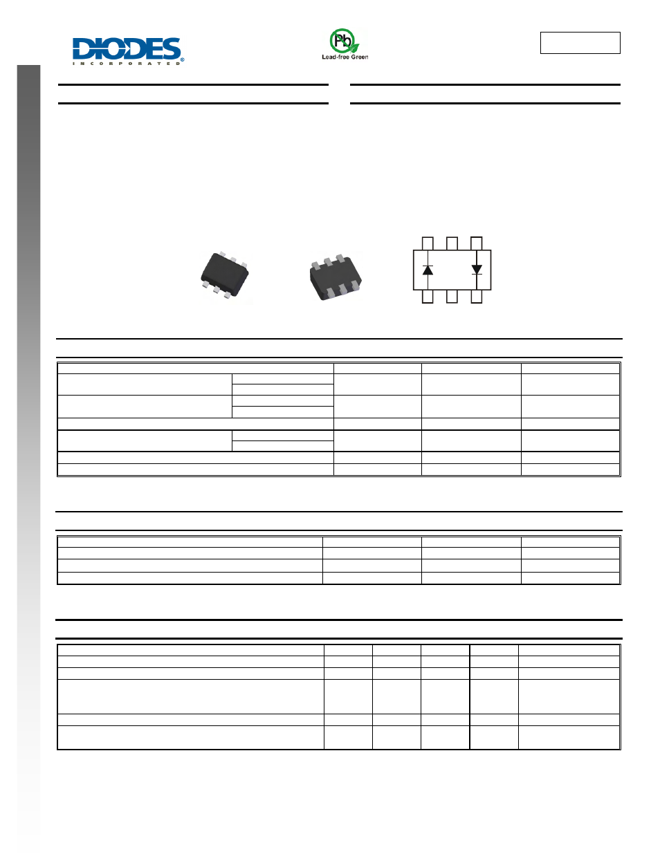
Top View
Bottom View
Device Schematic
1
2
3
6
5
4