Diodes BAT54DW User Manual
Bat54dw, Features, Mechanical data
BAT54DW
Document number: DS30107 Rev. 11 - 2
1 of 3
www.diodes.com
July 2008
© Diodes Incorporated
BAT54DW
DUAL SURFACE MOUNT SCHOTTKY BARRIER DIODE
Features
•
Low Forward Voltage Drop
•
Fast Switching
•
Ultra-Small Surface Mount Package
•
PN Junction Guard Ring for Transient and ESD Protection
•
Lead Free/RoHS Compliant (Note 3)
•
"Green" Device (Note 4 and 5)
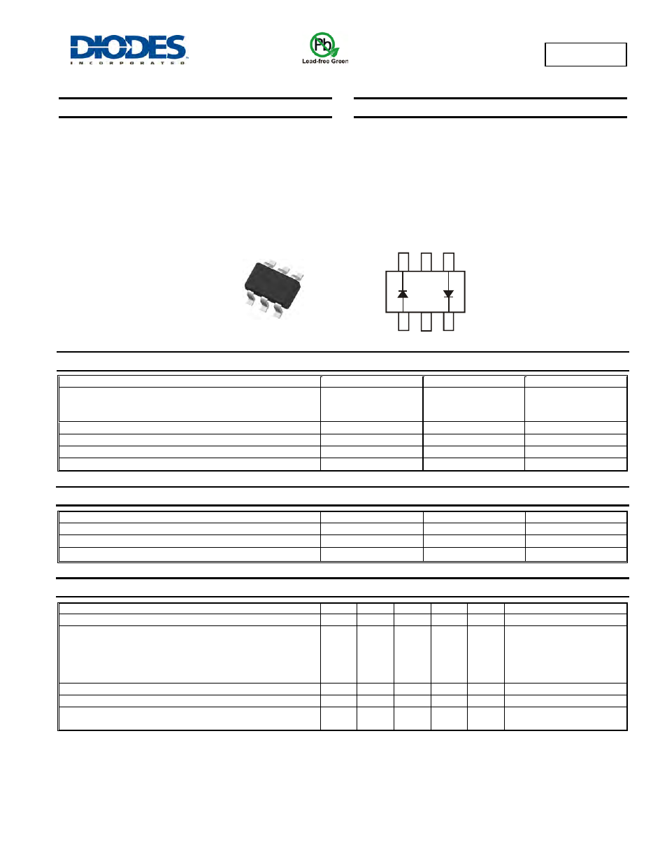
Mechanical Data
•
Case: SOT-363
•
Case Material: Molded Plastic. UL Flammability Classification
Rating 94V-0
•
Moisture Sensitivity: Level 1 per J-STD-020D
•
Terminals: Solderable per MIL-STD-202, Method 208
•
Lead Free Plating (Matte Tin Finish annealed over Alloy 42
leadframe).
•
Terminal Connections: See Diagram
•
Marking Information: See Page 2
•
Ordering Information: See Page 2
•
Weight: 0.006 grams (approximate)
A
2
C
1
NC
NC
C
2
A
1
Top View
Device Schematic
Maximum Ratings
@T
A
= 25°C unless otherwise specified
Characteristic
Symbol
Value
Unit
Peak Repetitive Reverse Voltage
Working Peak Reverse Voltage
DC Blocking Voltage
V
RRM
V
RWM
V
R
30
V
Average Rectified Forward Current
I
O
100
mA
Forward Continuous Current (Note 1)
I
F
200
mA
Repetitive Peak Forward Current (Note 1)
I
FRM
300
mA
Forward Surge Current (Note 1)
@ t < 1.0s
I
FSM
600
mA
Thermal Characteristics
Characteristic
Symbol
Value
Unit
Power Dissipation (Note 1)
P
D
200
mW
Thermal Resistance, Junction to Ambient Air (Note 1)
R
θJA
625
°C/W
Operating and Storage Temperature Range
T
J
, T
STG
-65 to +125
°C
Electrical Characteristics
@T
A
= 25°C unless otherwise specified
Characteristic
Symbol
Min
Typ
Max
Unit
Test Condition
Reverse Breakdown Voltage (Note 2)
V
(BR)R
30
⎯
⎯
V
I
RS
= 100
μA
Forward Voltage
V
F
⎯
⎯
240
320
400
500
1000
mV
I
F
= 0.1mA
I
F
= 1mA
I
F
= 10mA
I
F
= 30mA
I
F
= 100mA
Reverse Leakage Current (Note 2)
I
R
⎯
⎯
2.0
μA
V
R
= 25V
Total Capacitance
C
T
⎯
⎯
10
pF
V
R
= 1.0V, f = 1.0MHz
Reverse Recovery Time
t
rr
⎯
⎯
5.0
ns
I
F
= 10mA through I
R
= 10mA
to I
R
= 1.0mA, R
L
= 100
Ω
Notes:
1. Device mounted on FR-4 PCB, 1 inch x 0.85 inch x 0.062 inch; pad layout as shown on Diodes Inc. suggested pad layout document AP02001, which
can be found on our website at http://www.diodes.com/datasheets/ap02001.pdf.
2. Short duration pulse test used to minimize self-heating effect.
3. No purposefully added lead.
4. Diodes Inc.'s "Green" policy can be found on our website at http://www.diodes.com/products/lead_free/index.php.
5. Product manufactured with Date Code 0627 (week 27, 2006) and newer are built with Green Molding Compound. Product manufactured prior to Date
Code 0627 are built with Non-Green Molding Compound and may contain Halogens or Sb2O3 Fire Retardants.