Diodes BAT54TW /ADW /CDW /SDW /BRW User Manual
Bat54tw /adw, Cdw /sdw /brw, Features
BAT54TW /ADW /
BAT54TW /ADW /CDW /SDW /BRW
Document number: DS30152 Rev. 16 - 2
1 of 3
www.diodes.com
July 2008
© Diodes Incorporated
CDW /SDW /BRW
SURFACE MOUNT SCHOTTKY BARRIER DIODE ARRAYS
Features
•
Low Forward Voltage Drop
•
Fast Switching
•
Ultra-Small Surface Mount Package
•
PN Junction Guard Ring for Transient and ESD Protection
•
Lead Free/RoHS Compliant (Note 2)
•
"Green" Device (Note 3 and 4)
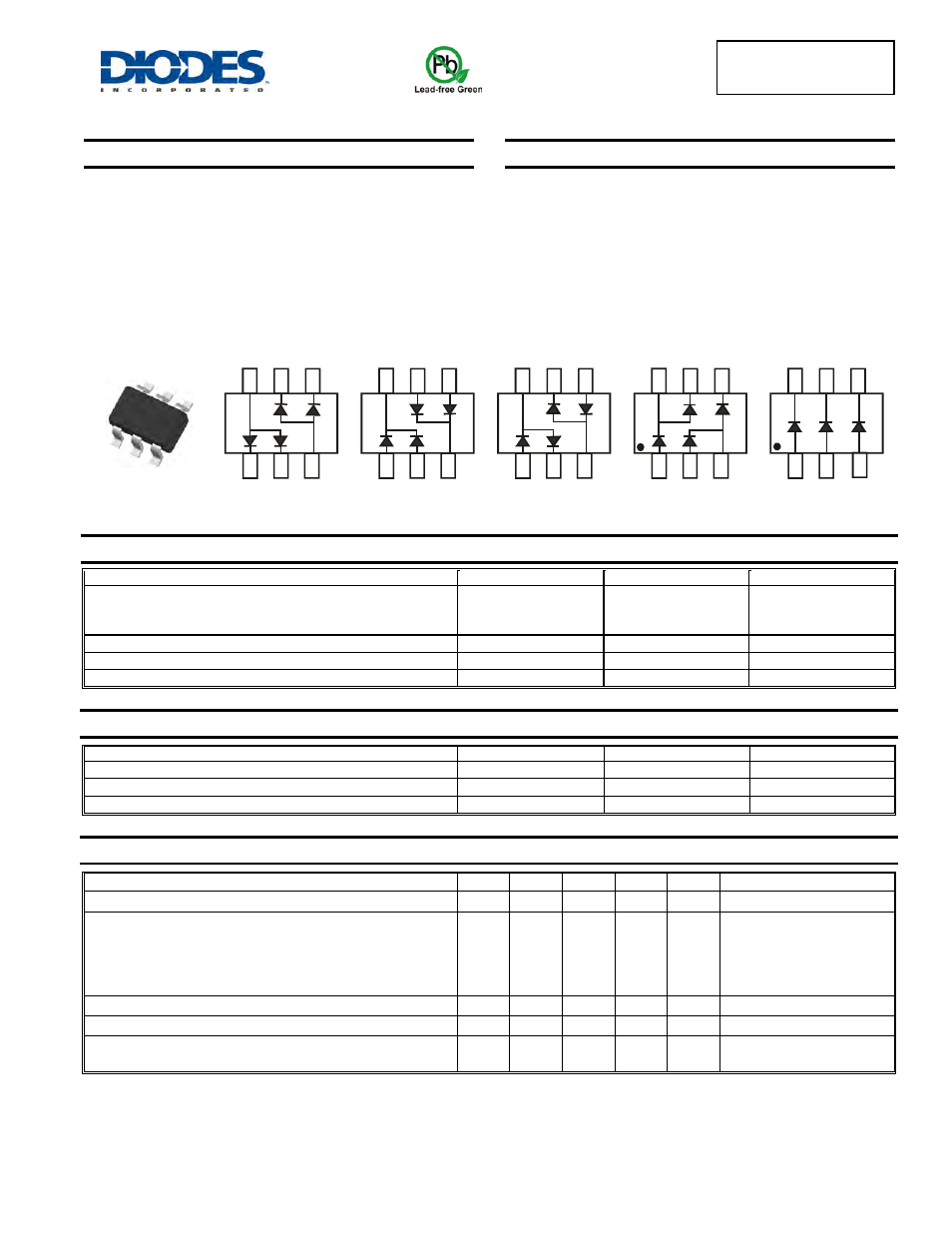
Mechanical Data
•
Case: SOT-363
•
Case Material: Molded Plastic. UL Flammability Classification
Rating 94V-0
•
Moisture Sensitivity: Level 1 per J-STD-020D
•
Terminals: Solderable per MIL-STD-202, Method 208
•
Lead Free Plating (Matte Tin Finish annealed over Alloy 42
leadframe).
•
Orientation: See Diagrams Below
•
Marking Information: See Page 3
•
Ordering Information: See Page 2
•
Weight: 0.006 grams (approximate)
A
1
A
2
C
2
C
1
C
2
C
1
C
1
C
2
A
2
A
1
A
2
A
1
AC
1
AC
2
C
2
A
1
A
2
C
1
AC
1
AC
2
C
1
A
1
C
2
A
2
C
1
A
3
C
2
A
1
C
3
A
2
Top
View BAT54ADW* BAT54CDW* BAT54SDW* BAT54BRW BAT54TW
*Symmetrical configuration, no orientation indicator.
Maximum Ratings
@T
A
= 25°C unless otherwise specified
Characteristic
Symbol
Value
Unit
Peak Repetitive Reverse Voltage
Working Peak Reverse Voltage
DC Blocking Voltage
V
RRM
V
RWM
V
R
30
V
Forward Continuous Current (Note 1)
I
F
200
mA
Repetitive Peak Forward Current (Note 1)
I
FRM
300
mA
Forward Surge Current (Note 1)
@ t < 1.0s
I
FSM
600
mA
Thermal Characteristics
Characteristic
Symbol
Value
Unit
Power Dissipation (Note 1)
P
D
200
mW
Thermal Resistance, Junction to Ambient Air (Note 1)
R
θJA
625
°C/W
Operating and Storage Temperature Range
T
J
, T
STG
-65 to +125
°C
Electrical Characteristics
@T
A
= 25°C unless otherwise specified
Characteristic
Symbol
Min
Typ
Max
Unit
Test Condition
Reverse Breakdown Voltage (Note 5)
V
(BR)R
30
⎯
⎯
V
I
R
= 100
μA
Forward Voltage (Note 5)
V
F
⎯
⎯
240
320
400
500
1000
mV
I
F
= 0.1mA
I
F
= 1mA
I
F
= 10mA
I
F
= 30mA
I
F
= 100mA
Reverse Leakage Current (Note 5)
I
R
⎯
⎯
2.0
μA
V
R
= 25V
Total Capacitance
C
T
⎯
⎯
10
pF
V
R
= 1.0V, f = 1.0MHz
Reverse Recovery Time
t
rr
⎯
⎯
5.0
ns
I
F
= 10mA through I
R
= 10mA
to I
R
= 1.0mA, R
L
= 100
Ω
Notes:
1. Device mounted on FR-4 PCB, 1 inch x 0.85 inch x 0.062 inch; pad layout as shown on Diodes Inc. suggested pad layout document AP02001, which
can be found on our website at http://www.diodes.com/datasheets/ap02001.pdf.
2. No purposefully added lead.
3. Diodes Inc.'s "Green" policy can be found on our website at http://www.diodes.com/products/lead_free/index.php.
4.
Code UO are built with Non-Green Molding Compound and may contain Halogens or Sb2O3 Fire Retardants
Product manufactured with Date Code UO (week 40, 2007) and newer are built with Green Molding Compound. Product manufactured prior to Date
5. Short duration pulse test used to minimize self-heating effect.