Diodes ZNBG3116 User Manual
Page 8
ZNBG3115
ZNBG3116
ISSUE 2 - JUNE 2006
8
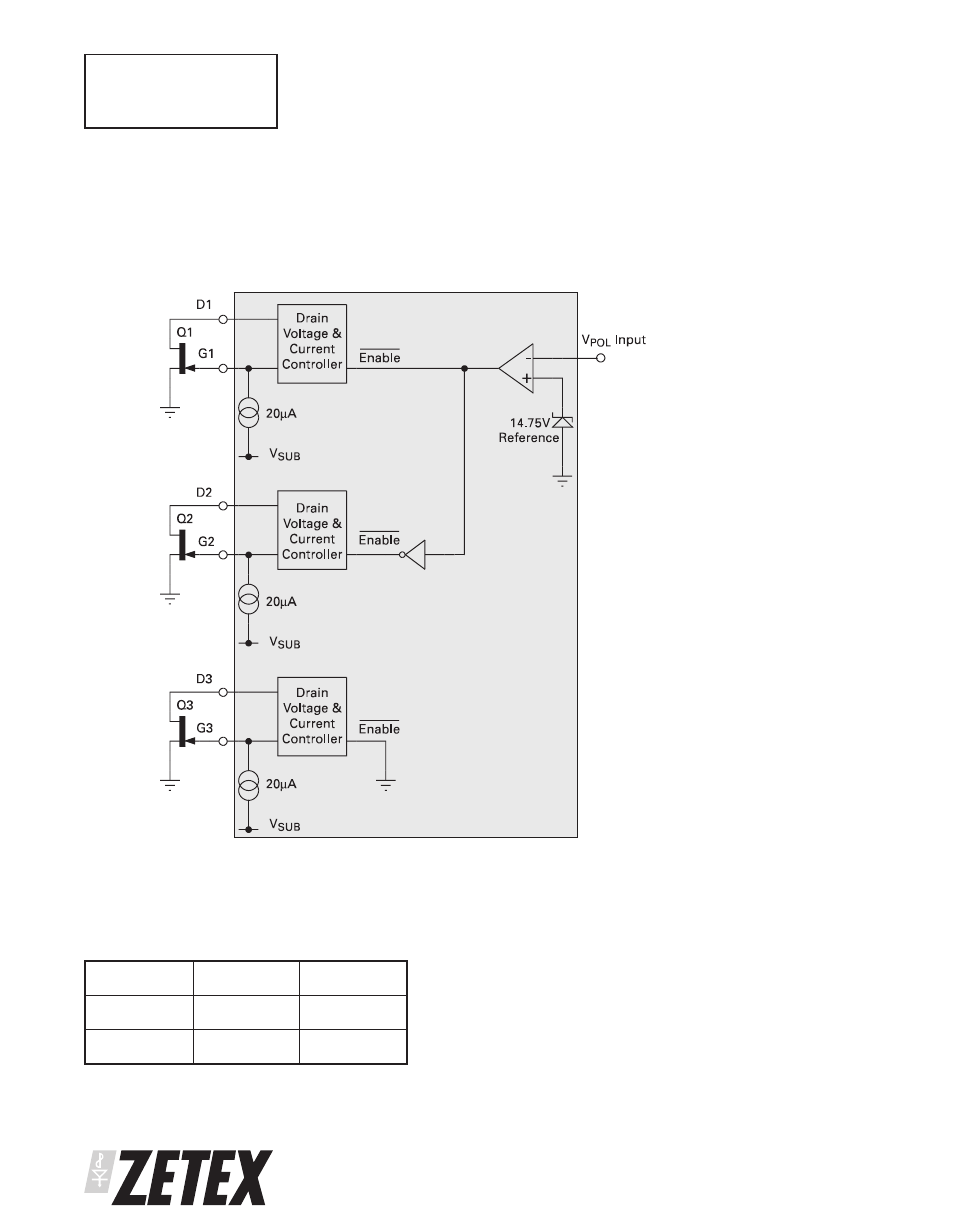
The following schematic shows the function of the V
POL
input. Only one of the two external FETs numberd Q1 and
Q2 are powered at any one time, their selection is controlled by the input V
POL
. This input is designed to be wired
to the power input of the LNB via a high value (10k) resistor. With the input voltage of the LNB set at or below 14V,
FET Q2 will be enabled. With the input voltage at or above 15.5V, FET Q1 will be enabled. The disabled FET has its
gate driven low and its drain terminal is switched open circuit. It is permissible to connect the drain pins D1 and
D2 together if required by the application circuit; this is done internally in the QSOP16 version. FET number Q3 is
always active regardless of the voltage applied to V
POL
.
Control Input Switch Function
Input Sense
Polarisation
Select
≤ 14 volts
Vertical
FET Q2
≥ 15.5 volts
Horizontal
FET Q1
QSOP 20 Version