Zlnb1001 – Diodes ZLNB1001 User Manual
Page 3
ZLNB1001
© Zetex Semiconductors plc 2005
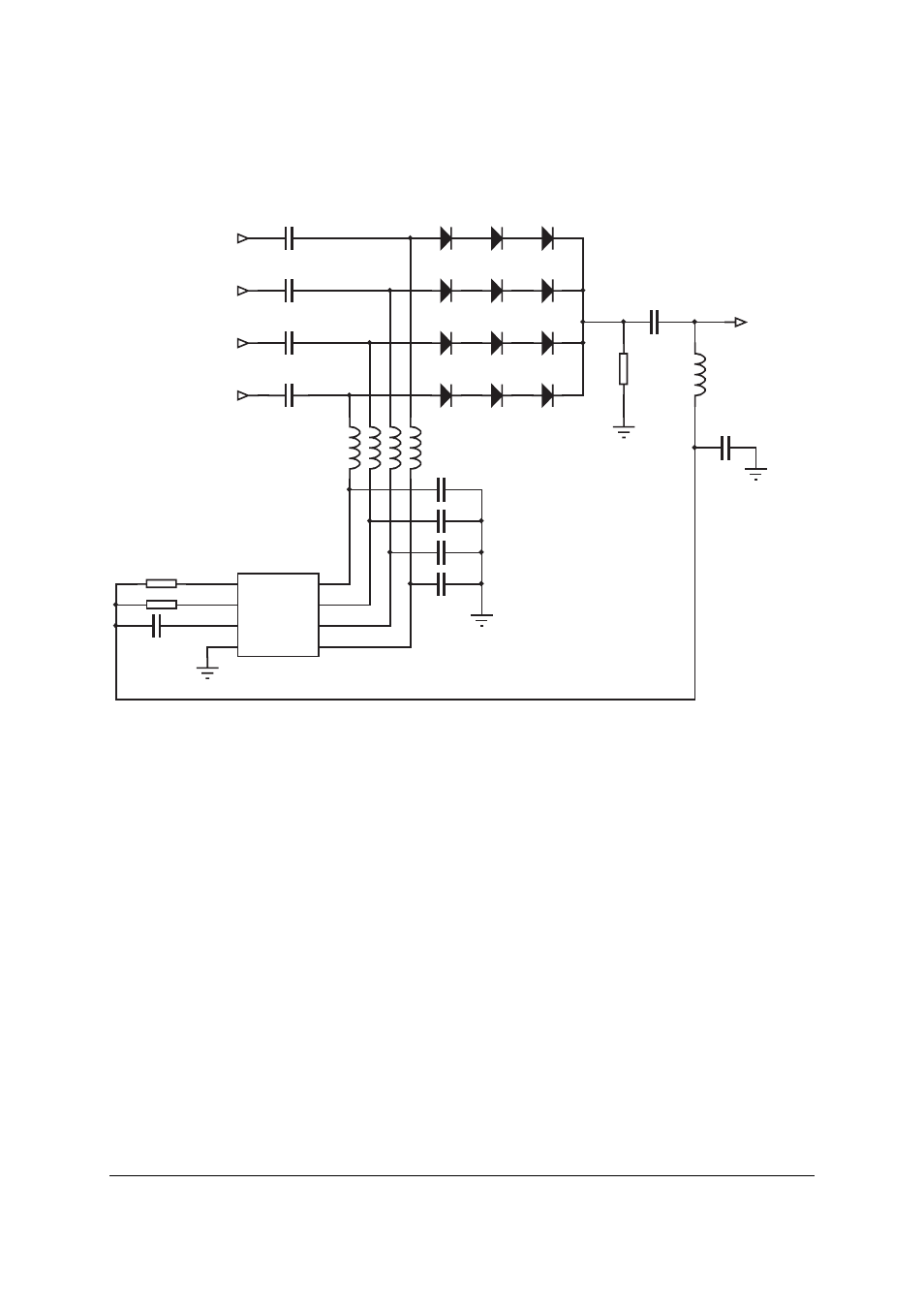
Typical application circuit using pin diodes
Application information
The schematic diagram above shows the typical application driving RF signal PIN diodes. Values
of suitable external components are shown. R1 R2 and C1 are required to achieve specified
operation. Values of other components are typical of the application. When one signal path is
selected according to the Truth Table, the selected signal diodes carry a forward current set by R3.
The other signal diodes are biased off, R3 providing a degree of reverse bias.
In order to limit the peak current in the device, it is recommended that the output decoupling
capacitor value, including C2, C3, C4 and C5, should not be excessive. Normally this total is
expected to be less than a few hundred pF in the intended application.
VIN
1
VOUT4
8
VPOL
2
VOUT3
7
VOUT2
6
VOUT1
5
FIN
3
GND
4
U1
ZLNB1001
Input, low band vert
Input, low band horiz
Input, high band vert
Input, high band horiz
IF out
R1
47R
R3
1k
typical
C2
47pF typical
R2
1k
C1
4.7nF
C3
47pF typical
C4
47pF typical
C5
47pF typical
C11 47pF typical