Zr431l, Electrical characteristics (at t, 25°c unless otherwise stated) – Diodes ZR431L User Manual
Page 4: Vδ δ
ZR431L
© Zetex Semiconductors plc 2008
Electrical characteristics (at T
amb
= 25°C unless otherwise stated)
DC Test circuits
Parameter
Symbol
Min.
Typ.
Max.
Unit
Conditions
Reference Voltage
2.5%
1.0%
V
ref
V
ref
1.209
1.228
1.24
1.24
1.271
1.252
V
V
I
L
= 10mA (Fig1), V
Z
= V
ref
Deviation of Reference
Input Voltage over
Temperature
V
dev
4.0
8.0
mV
I
L
= 10mA, V
Z
= V
ref
T
a
= full range (Fig 1)
Ratio of the change in
Reference Voltage to the
change in Cathode
Voltage)
0.5
2.0
mV/V
V
Z
from V
ref
to 10V
I
Z
= 10mA (Fig2)
Reference Input Current
I
ref
0.02
0.11
0.4
A
R1 = 10k, R2 = O/C,
l
L
= 10mA (fig2)
Deviation of Reference
Input Current over
Temperature
⌬I
ref
0.02
0.2
A
R1 = 10k, R2 = O/C,
I
L
= 10mA T
a
= full
range (Fig2)
Minimum Cathode
Current for Regulation
I
Zmin
30
100
A
Off-state Current
I
Zoff
10
30
A
V
Z
= 10V, V
ref
= 0V
(Fig3)
Dynamic Output
Impedance
R
Z
0.25
2
Ω
V
Z
= V
ref
(Fig1), f = 0Hz,
I
L
= 10mA
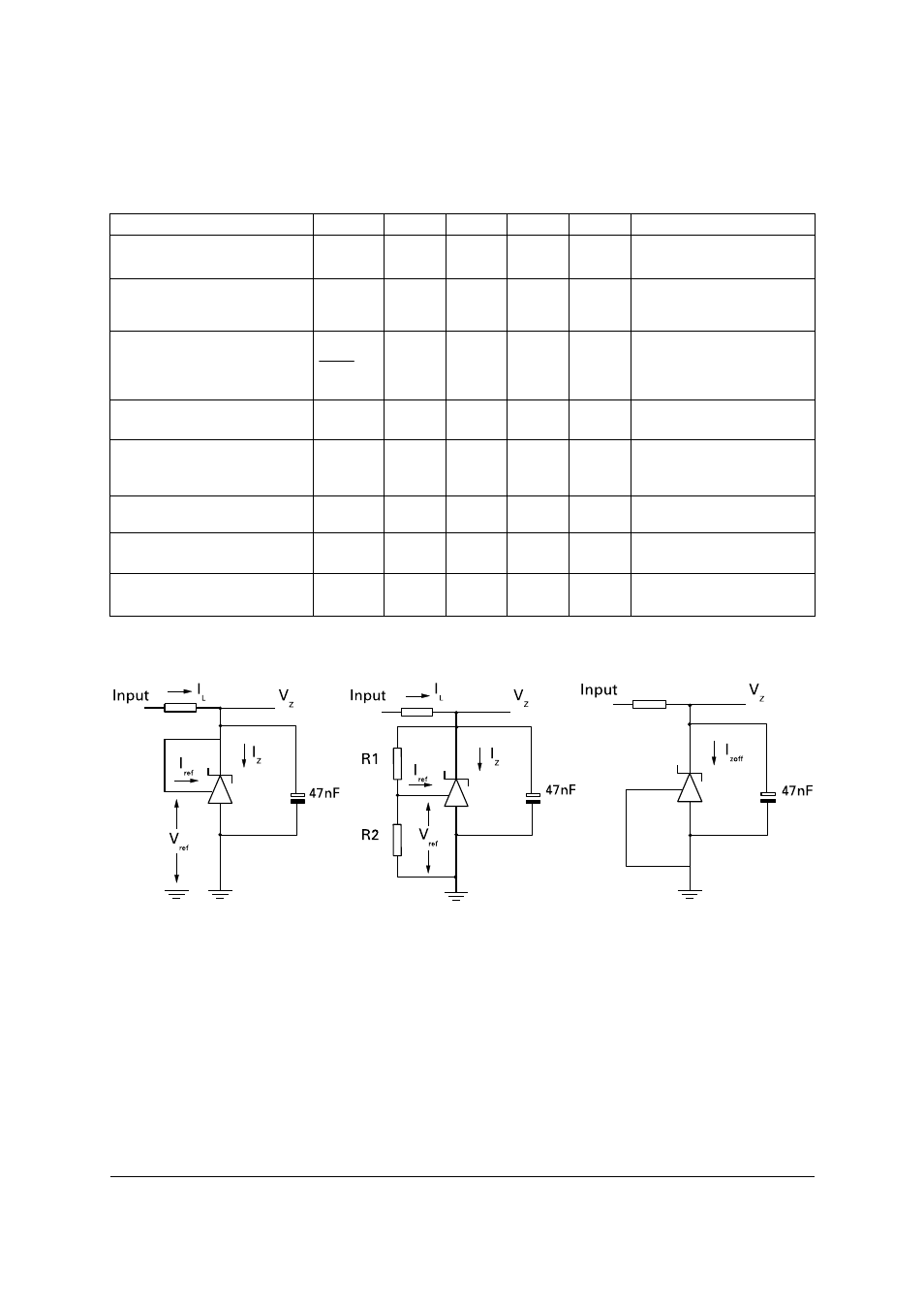
Fig 1 - Test Circuit for V
Z
= V
ref
Fig 2 - Test Circuit for V
Z
> V
ref
Fig 3 - Test Circuit for Off State
current
Z
ref
V
V
Δ
Δ