Electrical characteristics – Diodes ZXCT1082/83/84/85/86/87 User Manual
Page 3
ZXCT1082/83/84/85/86/87
ZXCT1082/83/84/85/86/87
Document number: DS32162 Rev. 2 - 2
3 of 13
June 2011
© Diodes Incorporated
A Product Line of
Diodes Incorporated
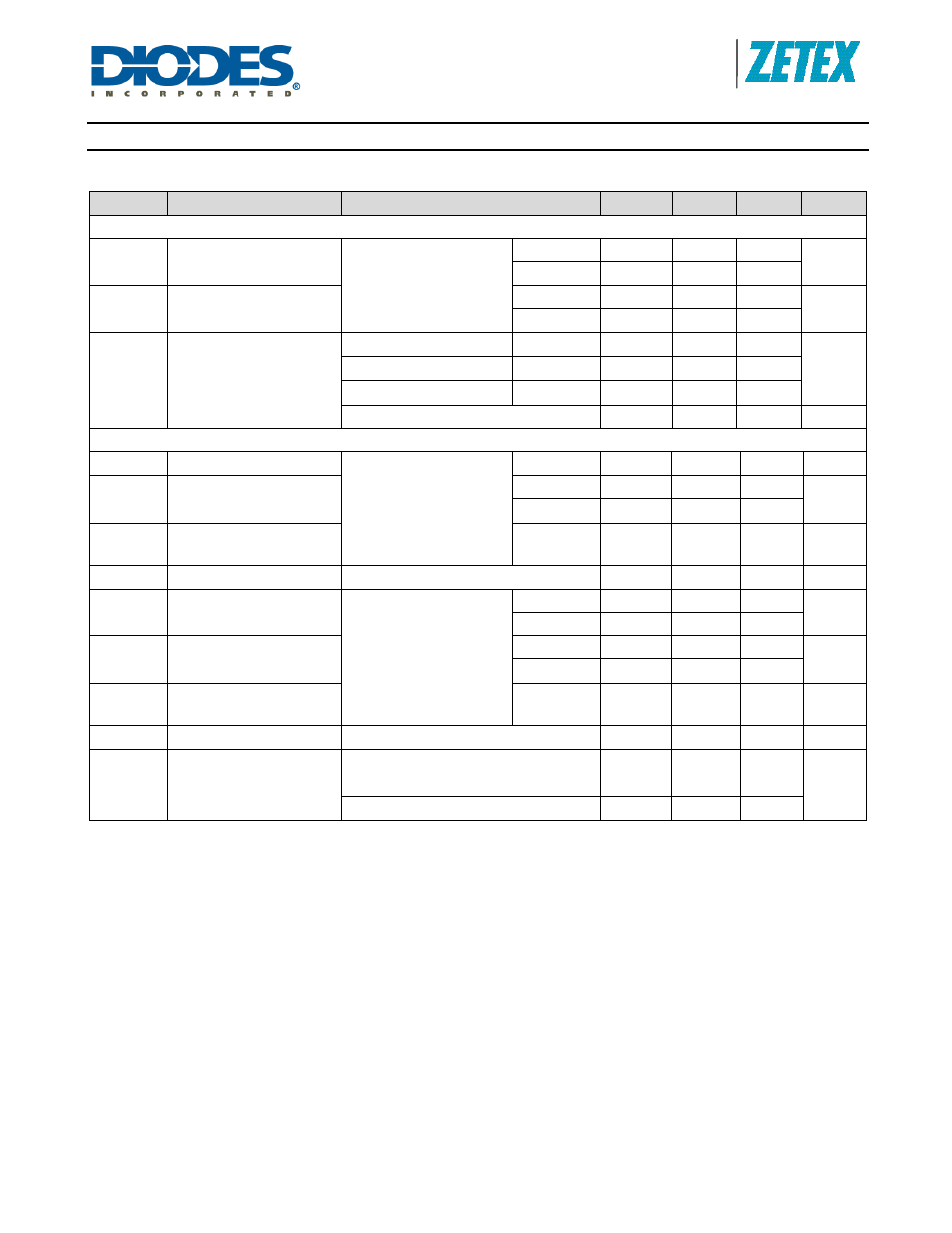
Electrical Characteristics
Test Conditions T
A
= 25
°C, V
S+
= 12V, V
CC
= 5 V, V
SENSE
1
= 100mV, ZXCT1082/3 R
GT
= 5k
Ω, R
G
= 125k
Ω; unless otherwise stated.
(FT = -40°C to +125°C)
Symbol
Parameter
Conditions
Min.
Typ.
Max.
Units
Input
I
S+
S+ input current
V
SENSE
= 0mV (Note 1)
1.7
µA
T
A
= FT
5
I
S-
S- input current
1.7
µA
T
A
= FT
5
V
IO
Input Offset Voltage
(Note 2)
V
SENSE
= 0mV
±0.2
±1
mV
ZXCT1082/3/4/5
T
A
= FT
±2.5
ZXCT1086/87
T
A
= FT
±3
Temperature co-efficient
±4
µV/K
Output
G
T
Transconductance
ZXCT1082/3
V
SENSE
= 10mV to 150mV
(Note 1, 3)
200
µA/V
G
T-ERR
Transconductance error
(Note 4)
-1
+1
%
T
A
= FT
-2 +2
G
T-TC
Transconductance
temperature co-efficient
T
A
= FT
10
nA/K
Z
OUT
Output impedance
ZXCT1082/3
1¦¦5
G
Ω¦¦pF
G
V
Gain
ZXCT1084/5/6/7
V
SENSE
= 10mV to 150mV
(Note 1)
1084/5
25
V/V
1086/7
50
G
V-ERR
Gain error (Note 4)
-1
+1
%
T
A
= FT
-2 +2
G
V-TC
Voltage gain temperature
co-efficient
T
A
= FT
100
ppm/K
Z
OUT
Output impedance
ZXCT1084/5/6/7
125
k
Ω
V
OUTH
Output relative to common
mode, V
S-
ZXCT1082/3
V
LOAD
- 1
V
LOAD
- 0.8
V
ZXCT1084/5/6/7
V
S-
- 1
V
S-
- 0.8
Notes:
1. For the ZXCT1082/83 V
SENSE
= “V
SUPPLY
” – “V
LOAD
“ where V
LOAD
is the load voltage or the lower potential side of the sense resistor.
For the ZXCT1083/84/85/86 V
SENSE
= “V
S+
” – “V
S-
“
2. V
IO
is extrapolated from measurements for the gain-error test.
3. For V
SENSE
> 10mV, the internal voltage-current converter is fully linear. This enables a true offset to be defined and used.
4. Gain or transconductance error is calculated by applying two values of V
SENSE
and calculating the error of the slope vs. the ideal.