Zxct1081, Electrical characteristics – Diodes ZXCT1081 User Manual
Page 3
ZXCT1081
ZXCT1081
Document number: DS32102 Rev. 1 - 2
3 of 11
March 2010
© Diodes Incorporated
A Product Line of
Diodes Incorporated
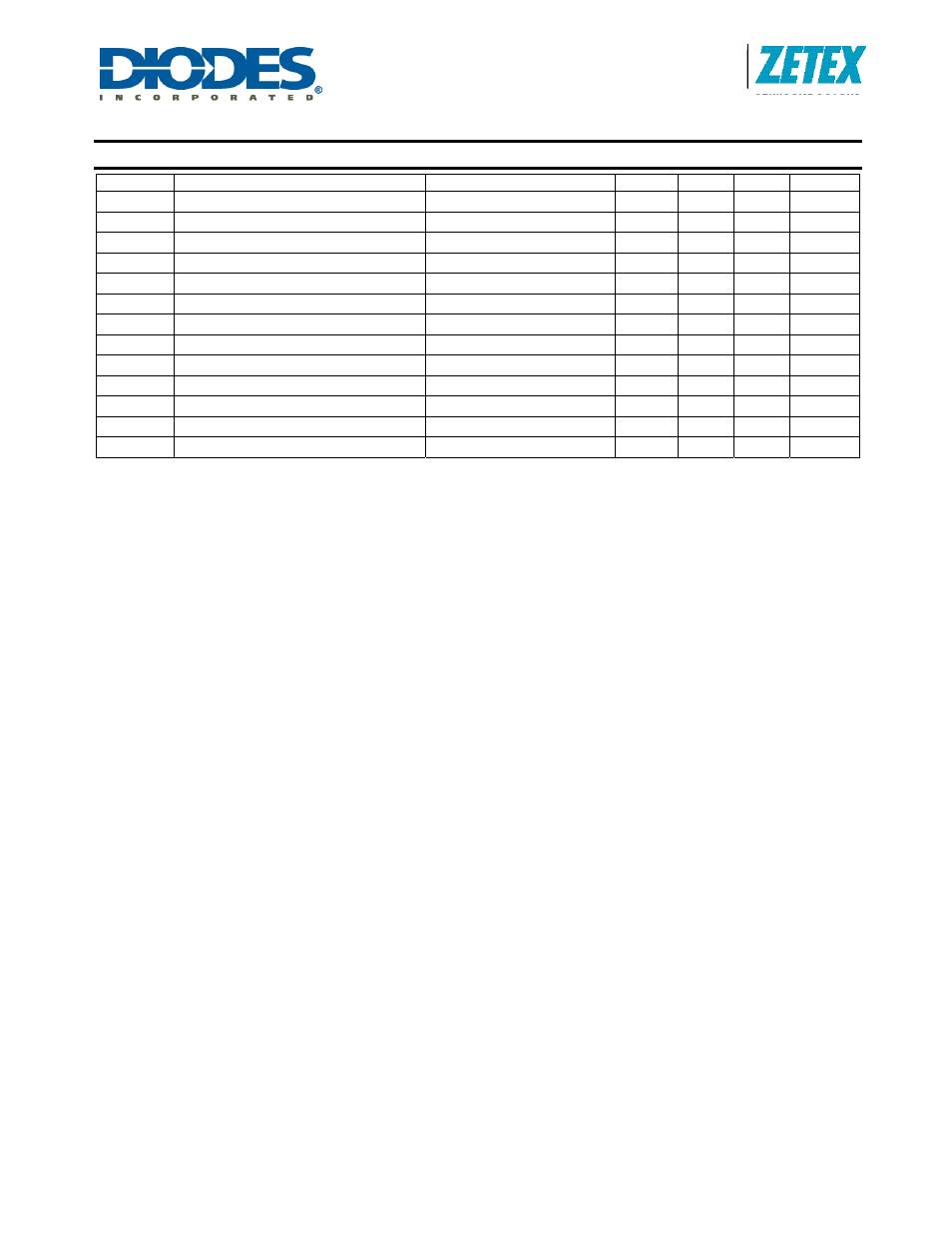
Electrical Characteristics
(Test conditions: T
A
= 25°C, V
IN
= 12V, V
CC
= 5V, V
SENSE
(a)
= 100mV unless otherwise stated)
Symbol Parameter Condition
Min.
Typ.
Max.
Unit
I
CC
VCC Supply Current
V
CC
= 12V
40 80
120 µA
I
SENSE
+
SENSE+ Input Current
15
30
60
µA
I
SENSE
-
SENSE- Input Current
10
40
80
nA
V
O(0)
Zero
V
SENSE
(a)
error
(b)
V
SENSE
(a)
= 0V
0
35
mV
V
O(10)
Output Offset Voltage
(c)
V
SENSE
(a)
= 10mV
-30 +30
mV
Gain
ΔV
OUT
/
ΔV
SENSE
(a)
V
SENSE
(a)
= 10mV to 150mV
9.95 10
10.05
V
OUT
TC
(d)
V
OUT
Variation with Temperature
30
ppm/°C
A
CC
Total Output Error -3
3
%
I
OH
Output Source Current
V
OUT
= 30mV
1 mA
I
OL
Output Sink Current
V
OUT
= +30mV
20 µA
PSRR
VCC Supply Rejection Ration
V
CC
= 4.5V to 12V
54 60 dB
CMRR
Common-Mode Sense Rejection Ratio V
IN
+ 40V to 3V
60 75 dB
BW
-3dB Small Signal Bandwidth
V
SENSE
(a)
(AC)
= 10mV
pp
50 kHz
Notes:
(a) VSENSE = "V
SENSE
+" - "V
SENSE
-"
(b) The ZXCT1081 operates from a positive power rail and the internal voltage-current converter current flow is unidirectional; these result in the
output offset voltage for V
SENSE
= 0V always being positive.
(c) For V
SENSE
> 10mV, the internal voltage-current converter is fully linear. This enables a true offset to be defined and used. V
O(10)
is expressed as
the variance about an output voltage of 100mV>.
(d)Temperature dependent measurements are extracted from characterization and simulation results.