Thermal resistance, Recommended operating conditions – Diodes ZXLD1356/ ZXLD1356Q User Manual
Page 4

ZXLD1356/ ZXLD1356Q
Document number: DS33470 Rev. 4 - 2
4 of 29
October 2012
© Diodes Incorporated
ZXLD1356/ ZXLD1356Q
A Product Line of
Diodes Incorporated
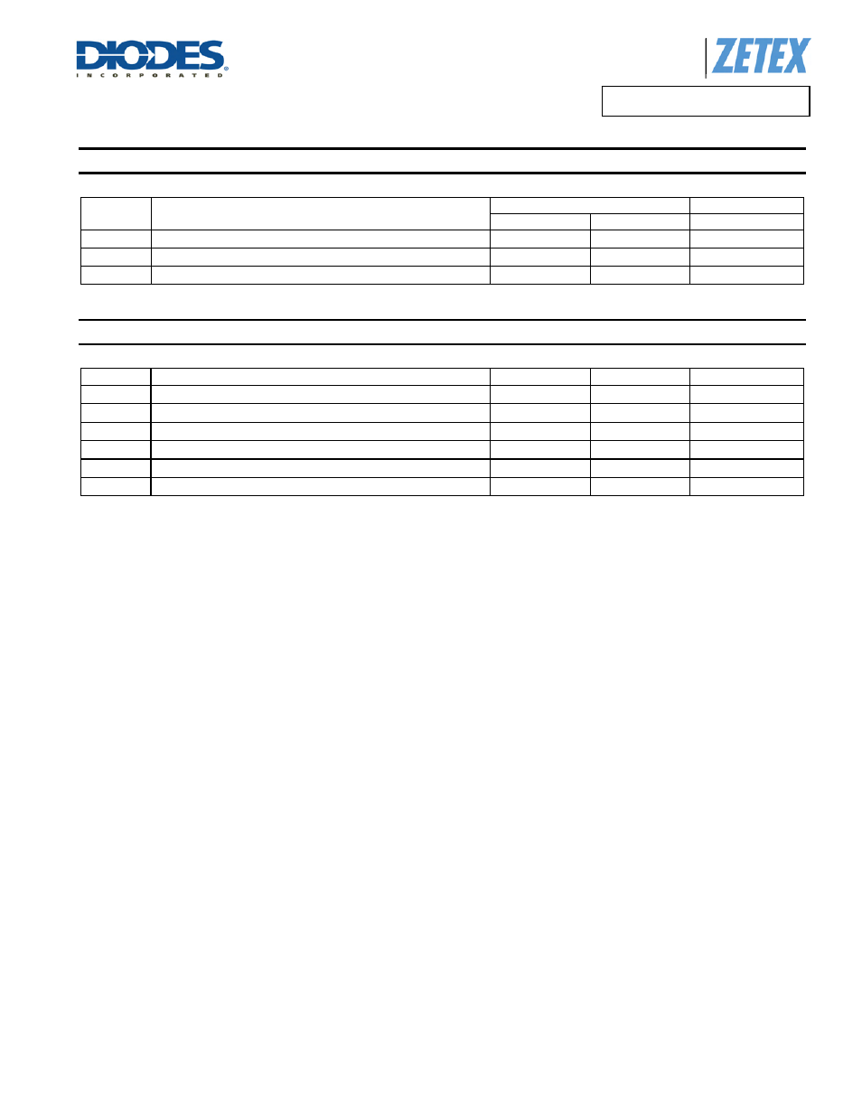
Thermal Resistance
Symbol Parameter
Rating Unit
TSOT25 V-DFN3030-6
θ
JA
Junction to Ambient
82
44
°C/W
Ψ
JB
Junction to Board
33
—
°C/W
θ
JC
Junction to Case
—
14
°C/W
Recommended Operating Conditions
(@T
A
= +25°C, unless otherwise specified.)
Symbol Parameter
Min
Max
Units
V
IN
Input voltage (Note 4)
6
60
V
t
OFFMIN
Minimum switch off-time
800
ns
t
ONMIN
Minimum switch on-time
800
ns
f
LX max
Recommended maximum operating frequency (Note 5)
625
kHz
D
LX
Duty cycle range
0.01
0.99
T
OP
Operating temperature range
-40
+125
°C
Notes: 4.
V
IN
> 16V to fully enhance output transistor. Otherwise out current must be derated - see graphs. Operation at low supply may cause excessive heating
due to increased on-resistance. Tested at 7V guaranteed for 6V by design.
5. ZXLD1356 will operate at higher frequencies but accuracy will be affected due to propagation delays.
