Zxld1320 – Diodes ZXLD1320 User Manual
Page 6
ZXLD1320
© Zetex Semiconductors plc 2008
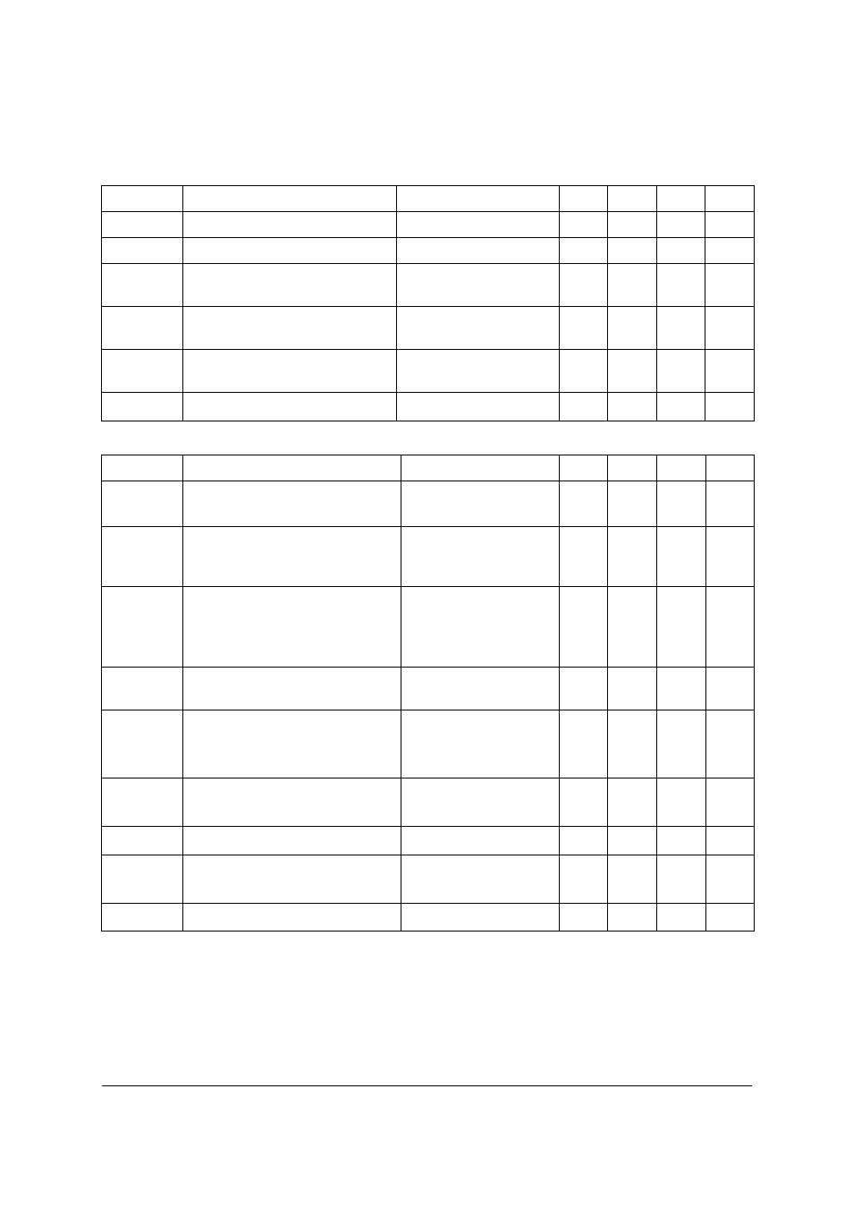
DC-DC converter output parameters
Switching NPN transistor
NOTES:
(b) Measured under pulse conditions.
(c) This current is measured via the collectors and emitters of the switch with these connected to ground (0V)
(d) Measured under pulse conditions. Peak Current = Ic
Symbol
Parameter
Conditions
Min
Typ
Max
Units
Toff(100)
Discharge pulse width
100% Output current
0.7
1.2
1.7
µs
Toff(10)
Discharge pulse width
10% Output current
4
8
12
µs
f
LXmax
Maximum operating
frequency
600
KHz
V
OH(POK)
POK flag high level output
voltage
4V
2
VIN
V
V
OL(POK)
POK flag low level output
voltage
Output sinking 1mA
0
0.4
V
T
(POK)
POK assertion delay time
Switch permanently on
300
500
700
µs
Symbol
Parameter
Conditions
Min
Typ
Max
Units
I
SW
Average continuous switch
current
1.5
A
I
BON(max)
Maximum base current into
switch transistor from internal
drive circuit
4V
30
50
70
mA
I
BON
Base current into switch
transistor using external
resistor (R
BASE
) from BIAS pin
to ground
R
BIAS
= 1680
Ω
10
mA
V
(BR)CE
Collector-Emitter breakdown
voltage
I
C
=10µA
20
V
V
CE(sat)
Collector-Emitter saturation
voltage
I
C
=0.1A, I
B
=10mA
I
C
=2A, I
B
=50mA
50
120
mV
mV
h
FE
Static forward current transfer
ratio
I
C
=200mA, V
CE
=2V
I
C
=2A, V
CE
=2V
209
116
C
OBO
Output capacitance
V
CB
=10V,f=1MHz
64
pF
t(on)
Turn-on time
Ic=0 to I
C
=2A
V
IN
=10V
30
ns
t(off)
Turn-off time
I
C
=2A to Ic<100µA
28
ns