Maximum ratings, Thermal characteristics, Electrical characteristics – Diodes SM12 User Manual
Page 2
SM12
Document number: DS35948 Rev. 6 - 2
2 of 5
November 2012
© Diodes Incorporated
SM12
ADVAN
CE I
N
F
O
RM
ATI
O
N
Maximum Ratings
(@T
A
= 25°C unless otherwise specified.)
Characteristic Symbol
Value
Unit
Conditions
Peak Pulse Power Dissipation
P
PP
300
W
8/20
μs, Per Fig. 3
Peak Pulse Current
I
PP
12 A
8/20
μs, Per Fig. 3
ESD Protection – Contact Discharge
V
ESD_Contact
±8 kV
Standard IEC 61000-4-2(ESD)
ESD Protection – Air Discharge
V
ESD_Air
±15 kV
Standard IEC 61000-4-2(ESD)
Electrical Fast Transient Current
I
EFT
40 A
Standard IEC 61000-4-4(EFT)
Thermal Characteristics
Characteristic Symbol
Value
Unit
Package Power Dissipation (Note 5)
P
D
250 mW
Thermal Resistance, Junction to Ambient (Note 5)
R
θJA
500
°C/W
Operating and Storage Temperature Range
T
J
, T
STG
-65 to +150
°C
Electrical Characteristics
(@T
A
= 25°C unless otherwise specified.)
Characteristic Symbol
Min
Typ
Max
Unit
Test
Conditions
Reverse Working Voltage
V
RWM
-
-
12.0
V
-
Reverse Current (Note 6)
I
R
- - 1.0
μA
V
R
= V
RWM
= 12.0V
Reverse Breakdown Voltage
V
BR
13.3
-
15.75
V I
R
= 1mA
Reverse Clamping Voltage
V
CL
- - 19 V
I
PP
= 1A, t
p
= 8/20
μs
Capacitance
C
T
- 95 -
pF
V
R
= 0V, f = 1MHz, Pin 1 to 3
Notes:
5. Device mounted on FR-4 PCB pad layout (2oz copper) as shown on Diodes, Inc. suggested pad layout AP02001, which can be found on our website at
6. Short duration pulse test used to minimize self-heating effect.
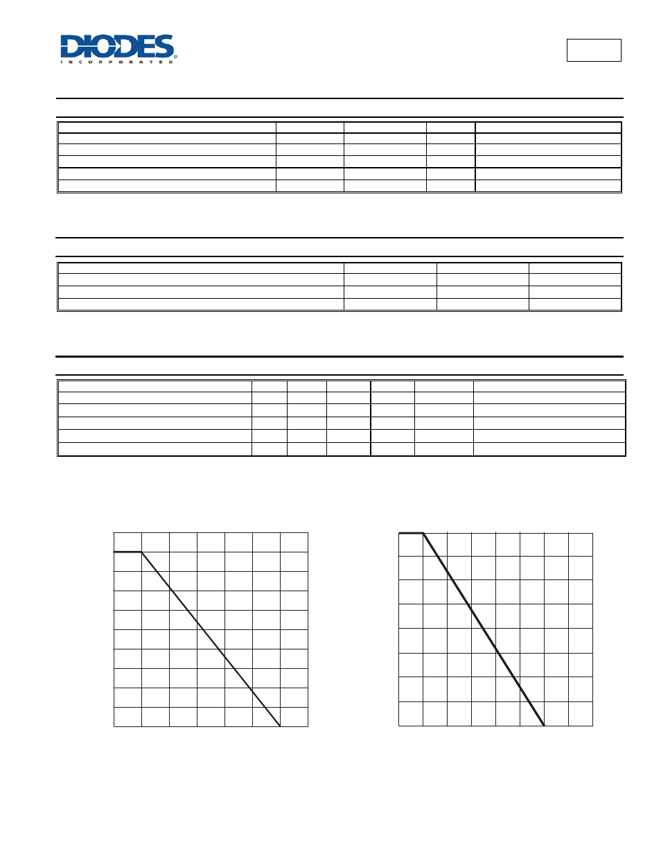
0
125
175
150
50
100
0
T , AMBIENT TEMPERATURE ( C)
Figure 1 Power Derating Curve
A
°
P
,
P
O
WE
R
DIS
S
IP
A
T
IO
N (
m
W
)
D
25
100
50
75
150
25
75
125
300
175
Note 5
250
200
0
50
25
50
75
100
125
150
P
EAK
P
U
LS
E
D
E
R
A
T
IN
G
%
O
F
P
EAK
PO
W
E
R O
R
CUR
RENT
T , AMBIENT TEMPERATURE (°C)
Figure 2 Power Dissipation vs. Ambient Temperature
A
0
100
25
75
175 200