Electrical characteristics – q2 p-channel, Zxmc3amc, A product line of diodes incorporated – Diodes ZXMC3AMC User Manual
Page 7
ZXMC3AMC
Document number: DS35088 Rev. 1 - 2
7 of 11
December 2010
© Diodes Incorporated
ZXMC3AMC
A Product Line of
Diodes Incorporated
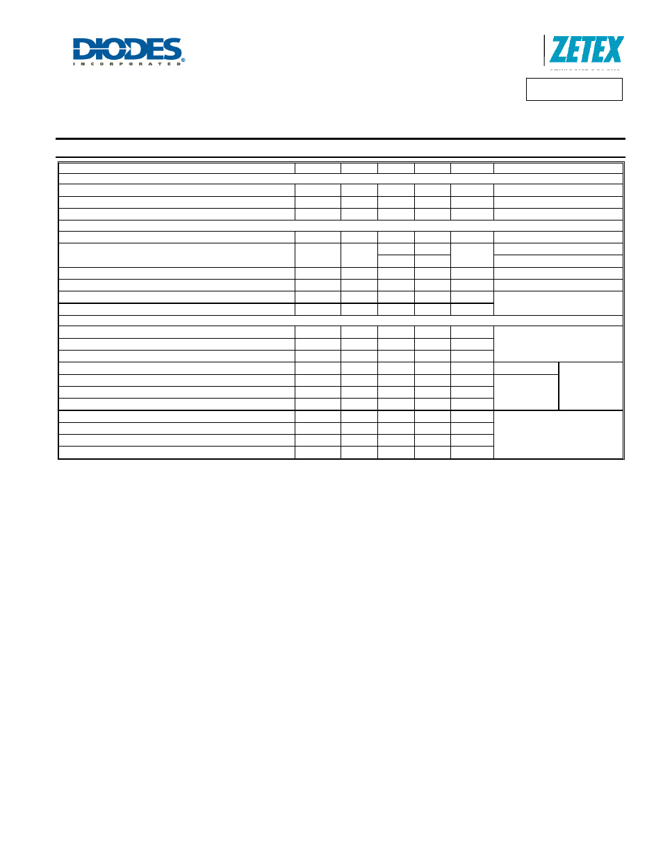
Electrical Characteristics – Q2 P-Channel
@T
A
= 25°C unless otherwise specified
Characteristic
Symbol
Min
Typ
Max
Unit
Test Condition
OFF CHARACTERISTICS
Drain-Source Breakdown Voltage
BV
DSS
-30 - - V
I
D
= -250
μA, V
GS
= 0V
Zero Gate Voltage Drain Current
I
DSS
- -
-0.5
μA
V
DS
= -30V, V
GS
= 0V
Gate-Source Leakage
I
GSS
- -
±100
nA
V
GS
= ±20V, V
DS
= 0V
ON CHARACTERISTICS
Gate Threshold Voltage
V
GS(th)
-1.0 - -3.0 V
I
D
= -250
μA, V
DS
= V
GS
Static Drain-Source On-Resistance (Note 13)
R
DS (ON)
-
0.150 0.210
Ω
V
GS
= -10V, I
D
= -1.4A
0.280 0.330
V
GS
= -4.5V, I
D
= -1.1A
Forward Transconductance (Note 13 & 14)
g
fs
- 2.48 -
S
V
DS
= -15V, I
D
= -1.4A
Diode Forward Voltage (Note 13)
V
SD
- -0.85
-0.95 V
I
S
= -1.1A, V
GS
= 0V
Reverse Recover Time (Note 14)
t
rr
- 18.6 -
ns
I
S
= -0.95A, di/dt = 100A/µs
Reverse Recover Charge (Note 14)
Q
rr
- 14.8 -
nC
DYNAMIC CHARACTERISTICS (Note 14)
Input Capacitance
C
iss
- 206 - pF
V
DS
= -15V, V
GS
= 0V,
f = 1.0MHz
Output Capacitance
C
oss
- 59.3 - pF
Reverse Transfer Capacitance
C
rss
- 49.2 - pF
Total Gate Charge (Note 15)
Q
g
- 3.8 - nC
V
GS
= -4.5V
V
DS
= -15V
I
D
= -1.4A
Total Gate Charge (Note 15)
Q
g
- 6.4 - nC
V
GS
= -10V
Gate-Source Charge (Note 15)
Q
gs
- 0.69 - nC
Gate-Drain Charge (Note 15)
Q
gd
- 2.0 - nC
Turn-On Delay Time (Note 15)
t
D(on)
- 1.5 - ns
V
DS
= -15V, I
D
= -1A
V
GS
= -10V, R
G
= 6
Ω
Turn-On Rise Time (Note 15)
t
r
- 2.8 - ns
Turn-Off Delay Time (Note 15)
t
D(off)
- 11.3 - ns
Turn-Off Fall Time (Note 15)
t
f
- 7.5 - ns
Notes:
13. Measured under pulsed conditions. Width
≤ 300µs. Duty cycle ≤ 2%.
14. For design aid only, not subject to production testing.
15. Switching characteristics are independent of operating junction temperature.