Electrical characteristics (at t, 25°c unless otherwise stated) – Diodes ZXMP2120G4 User Manual
Page 3
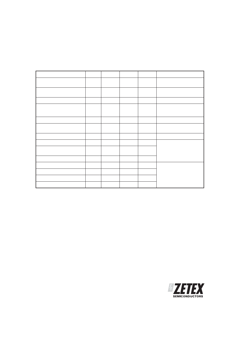
ZXMP2120G4
ISSUE 2 - SEPTEMBER 2006
3
ELECTRICAL CHARACTERISTICS (at T
amb
= 25°C unless otherwise stated)
PARAMETER
SYMBOL
MIN.
MAX.
UNIT
CONDITIONS
Drain-Source
Breakdown Voltage
BV
DSS
-200
V
I
D
=-1mA, V
GS
=0V
Gate-Source Threshold
Voltage
V
GS(th)
-1.5
-3.5
V
I
D
=-1mA, V
DS
= V
GS
Gate-Body Leakage
I
GSS
20
nA
V
GS
=
Ϯ20V, V
DS
=0V
Zero Gate Voltage Drain
Current
I
DSS
-10
-100
µA
µA
V
DS
=-200 V, V
GS
=0V
V
DS
=-160 V, V
GS
=0V,
T=125°C
(2)
On-State Drain Current
(1)
I
D(on)
-300
mA
V
DS
=-25 V, V
GS
=-10V
Static Drain-Source On-State
Resistance
(1)
R
DS(on)
25
Ω
V
GS
=-10V, I
D
=-150mA
Forward Transconductance
(1)(2)
g
fs
50
mS
V
DS
=-25V, I
D
=-150mA
Input Capacitance
(2)
C
iss
100
pF
Common Source Output
Capacitance
(2)
C
oss
25
pF
V
DS
=-25V, V
GS
=0V, f=1MHz
Reverse Transfer Capacitance
(2)
C
rss
7
pF
Turn-On Delay Time
(2)(3)
t
d(on)
7
ns
V
DD
-25V, I
D
=-150mA
Rise Time
(2)(3)
t
r
15
ns
Turn-Off Delay Time
(2)(3)
t
d(off)
12
ns
Fall Time
(2)(3)
t
f
15
ns
(1) Measured under pulsed conditions. Width=300
µs. Duty cycle ®2%
(2) Sample test.
(3) Switching times measured with 50
Ω source impedance and <5ns rise time on a pulse generator