Zvp4525g – Diodes ZVP4525G User Manual
Page 2
ZVP4525G
S E M I C O N D U C T O R S
ISSUE 4 - JUNE 2004
2
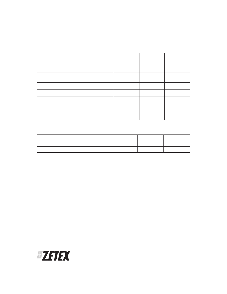
THERMAL RESISTANCE
PARAMETER
SYMBOL
VALUE
UNIT
Junction to ambient
(a)
R
θJA
63
°C/W
Junction to ambient
(b)
R
θJA
26
°C/W
NOTES:
(a) For a device surface mounted on 25mm x 25mm FR4 PCB with high coverage of single sided 1oz copper, in still air conditions
(b) For a device surface mounted on FR4 PCB measured at t
р5 secs.
(c) Repetitive rating - pulse width limited by maximum junction temperature. Refer to Transient Thermal Impedance graph.
ABSOLUTE MAXIMUM RATINGS.
PARAMETER
SYMBOL
LIMIT
UNIT
Drain-source voltage
V
DSS
250
V
Gate source voltage
V
GS
±40
V
Continuous drain current
(V
GS
=10V; TA=25°C)
(a)
(V
GS
=10V; TA=70°C)
(a)
I
D
I
D
-265
-212
mA
mA
Pulsed drain current
(c)
I
DM
-1
A
Continuous source current (body diode)
I
S
-0.75
A
Pulsed source current (body diode)
I
SM
-1
A
Power dissipation at T
A
=25°C
(a)
Linear derating factor
P
D
2
16
W
mW/°C
Operating and storage temperature range
T
j
:
T
stg
-55 to +150
°C
NB High voltage applications
For high voltage applications, the appropriate industry sector guidelines should be considered with regard to
voltage spacing between conductors.