Diodes ZVP4424A User Manual
Zvp4424c, Zvp4424a, P-channel enhancement mode vertical dmos fet
P-CHANNEL ENHANCEMENT
MODE VERTICAL DMOS FET
ISSUE 2 SEPTEMBER 94
FEATURES
* 240 Volt V
DS
* R
DS(on)
=9
Ω
* Low threshold
APPLICATIONS
* Electronic Hook Switch
REFER TO ZVP4424A FOR GRAPHS
ABSOLUTE MAXIMUM RATINGS.
PARAMETER
SYMBOL
VALUE
UNIT
Drain-Source Voltage
V
DS
-240
V
Continuous Drain Current at T
amb
=25°C
I
D
-200
mA
Pulsed Drain Current
I
DM
-1
A
Gate Source Voltage
V
GS
±
40
V
Power Dissipation at T
amb
=25°C
P
tot
750
mW
Operating and Storage Temperature Range
T
j
:T
stg
-55 to +150
°C
ELECTRICAL CHARACTERISTICS (at T
amb
= 25°C unless otherwise stated).
PARAMETER
SYMBOL MIN. TYP
MAX. UNIT CONDITIONS.
Drain-Source Breakdown
Voltage
BV
DSS
-240
V
I
D
=-1mA, V
GS
=0V
Gate-Source Threshold
Voltage
V
GS(th)
-0.7
-1.4
-2.0
V
ID=-1mA, V
DS
= V
GS
Gate-Body Leakage
I
GSS
100
nA
V
GS
=
±
40V, V
DS
=0V
Zero Gate Voltage Drain
Current
I
DSS
-10
-100
µ
A
µ
A
V
DS
=-240 V, V
GS
=0
V
DS
=-190V, V
GS
=0V, T=125°C
On-State Drain Current
I
D(on)
-0.75 -1.0
A
V
DS
=-10 V, V
GS
=-10V
Static Drain-Source
On-State Resistance
R
DS(on)
7.1
8.8
9
11
Ω
Ω
V
GS
=-10V,I
D
=-200mA
V
GS
=-3.5V,I
D
=-100mA
Forward
Transconductance (1) (2)
g
fs
125
mS
V
DS
=-10V,I
D
=-0.2A
Input Capacitance (2)
C
iss
100
200
pF
V
DS
=-25V, V
GS
=0V, f=1MHz
Common Source Output
Capacitance (2)
C
oss
18
25
pF
Reverse Transfer
Capacitance (2)
C
rss
5
15
pF
Turn-On Delay Time (2)(3)
t
d(on)
8
15
ns
V
DD
≈−
50V, I
D
=-0.25A,
V
GEN
=-10V
Rise Time (2)(3)
t
r
8
15
ns
Turn-Off Delay Time (2)(3)
t
d(off)
26
40
ns
Fall Time (2)(3)
t
f
20
30
ns
(1) Measured under pulsed conditions. Width=300
µ
s. Duty cycle
≤
2% (2) Sample test.
(3) Switching times measured with 50
Ω
source impedance and <5ns rise time on a pulse generator
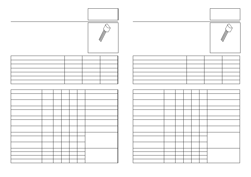
E-Line
TO92 Compatible
3-439
ZVP4424C
3-436
G
D
S
P-CHANNEL ENHANCEMENT
MODE VERTICAL DMOS FET
ISSUE 2 SEPTEMBER 94
FEATURES
* 240 Volt V
DS
* R
DS(on)
=9
Ω
* Low threshold
APPLICATIONS
* Electronic Hook Switch
ABSOLUTE MAXIMUM RATINGS.
PARAMETER
SYMBOL
VALUE
UNIT
Drain-Source Voltage
V
DS
-240
V
Continuous Drain Current at T
amb
=25°C
I
D
-200
mA
Pulsed Drain Current
I
DM
-1
A
Gate Source Voltage
V
GS
±
40
V
Power Dissipation at T
amb
=25°C
P
tot
750
mW
Operating and Storage Temperature Range
T
j
:T
stg
-55 to +150
°C
ELECTRICAL CHARACTERISTICS (at T
amb
= 25°C unless otherwise stated).
PARAMETER
SYMBOL MIN. TYP
MAX. UNIT CONDITIONS.
Drain-Source Breakdown
Voltage
BV
DSS
-240
V
I
D
=-1mA, V
GS
=0V
Gate-Source Threshold
Voltage
V
GS(th)
-0.7
-1.4
-2.0
V
ID=-1mA, V
DS
= V
GS
Gate-Body Leakage
I
GSS
100
nA
V
GS
=
±
40V, V
DS
=0V
Zero Gate Voltage Drain
Current
I
DSS
-10
-100
µ
A
µ
A
V
DS
=-240 V, V
GS
=0
V
DS
=-190V, V
GS
=0V, T=125°C
On-State Drain Current
I
D(on)
-0.75 -1.0
A
V
DS
=-10 V, V
GS
=-10V
Static Drain-Source
On-State Resistance
R
DS(on)
7.1
8.8
9
11
Ω
Ω
V
GS
=-10V,I
D
=-200mA
V
GS
=-3.5V,I
D
=-100mA
Forward
Transconductance (1) (2)
g
fs
125
mS
V
DS
=-10V,I
D
=-0.2A
Input Capacitance (2)
C
iss
100
200
pF
V
DS
=-25V, V
GS
=0V, f=1MHz
Common Source Output
Capacitance (2)
C
oss
18
25
pF
Reverse Transfer
Capacitance (2)
C
rss
5
15
pF
Turn-On Delay Time (2)(3)
t
d(on)
8
15
ns
V
DD
≈−
50V, I
D
=-0.25A,
V
GEN
=-10V
Rise Time (2)(3)
t
r
8
15
ns
Turn-Off Delay Time (2)(3)
t
d(off)
26
40
ns
Fall Time (2)(3)
t
f
20
30
ns
(1) Measured under pulsed conditions. Width=300
µ
s. Duty cycle
≤
2% (2) Sample test.
(3) Switching times measured with 50
Ω
source impedance and <5ns rise time on a pulse generator
E-Line
TO92 Compatible
ZVP4424A
D
G
S