Maximum ratings, Thermal characteristics, Electrical characteristics – Diodes ZVP2106G User Manual
Page 2
ZVP2106G
Document number: DS33393 Rev. 4 - 2
2 of 6
April 2014
© Diodes Incorporated
ZVP2106G
ADVAN
CE I
N
F
O
RM
ATI
O
N
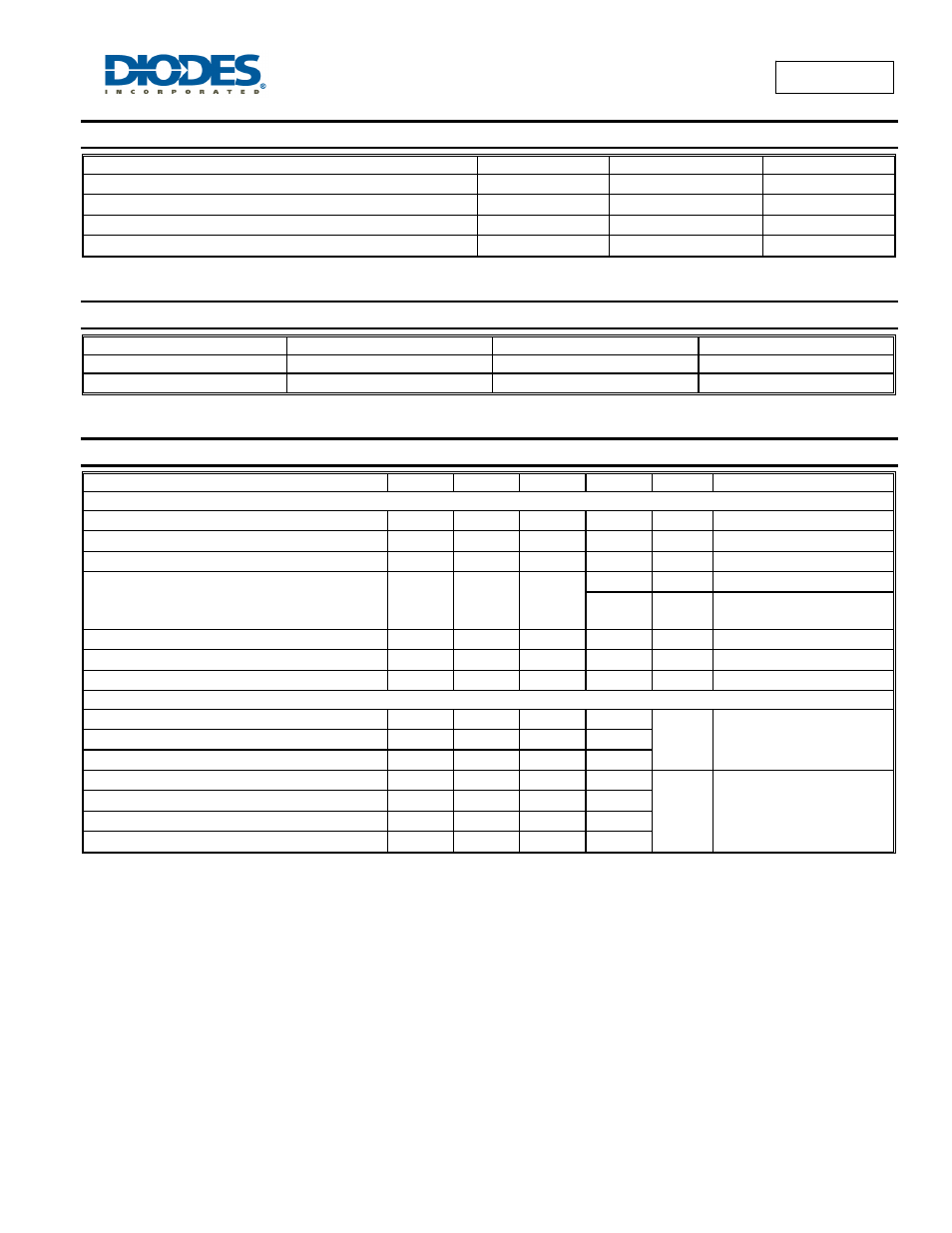
Maximum Ratings
(@T
A
= +25°C, unless otherwise specified.)
Characteristic Symbol
Value
Units
Drain-Source Voltage
V
DS
-60 V
Gate Source Voltage
V
GS
±
20
V
Continuous Drain Current
I
D
-450 M
A
Pulsed Drain Current
I
DM
-4 A
Thermal Characteristics
(@T
A
= +25°C, unless otherwise specified.)
Characteristic Symbol
Value
Units
Power Dissipation
P
TOT
2 W
Storage Temperature Range
T
STG
-55 to +150
°C
Electrical Characteristics
(@T
A
= +25°C, unless otherwise specified.)
Characteristic Symbol
Min
Typ
Max
Unit
Test
Condition
Static Characteristics
Drain-Source Breakdown Voltage
BV
DSS
-60
—
— V
I
D
= -1mA, V
GS
= 0V
Gate-Source Threshold Voltage
V
GS(th)
-1.5
—
-3.5 V
I
D
= -1mA, V
DS
= V
GS
Gate-Body Leakage
I
GSS
—
—
20 nA
V
GS
= ±20V, V
DS
= 0V
Zero Gate Voltage Drain Current
I
DSS
— —
-0.5 µA
V
DS
= -60V, V
GS
= 0V
-100 µA
V
DS
= -48V, V
GS
= 0V,
T= +125
°C (Note 6)
On-State Drain Current (Note 5)
I
D(on)
-1
—
— A
V
DS
= -18V, V
GS
= -10V
Static Drain-Source On-State Resistance (Note 5)
R
DS(on)
—
—
5
Ω
V
GS
= -10V, I
D
= -500mA
Forward Transconductance (Note 5 & 6)
g
fS
150
—
— mS
V
DS
= -18V, I
D
= -500mA
Dynamic Characteristics (Note 6)
Input Capacitance
C
iss
— — 100
pF
V
DS
= -18V, V
GS
= 0V, f=1MHz
Common Source Output Capacitance
C
oss
— — 60
Reverse Transfer Capacitance
C
rss
— — 20
Turn-On Delay Time (Note 7)
t
d(on)
— — 7
ns
V
DD
= -18V, I
D
= -500mA
Rise Time (Note 7)
t
r
— — 5
Turn-Off Delay Time (Note 7)
t
d(off)
— — 12
Fall Time (Note 7)
f
f
— — 15
Notes:
5. Measured under pulsed conditions. Width=300µ
s
. Duty cycle ≦ 2%.
6. Sample test.
7. Switching times measured with 50Ω source impedance and <5ns rise time on a pulse generator.